Semiconductor device with isolated body portion

A semiconductor, main body technology, used in semiconductor devices, semiconductor/solid-state device manufacturing, electrical solid-state devices, etc.

Active Publication Date: 2014-11-05
INTEL CORP
View PDF5 Cites 6 Cited by
  • Summary
  • Abstract
  • Description
  • Claims
  • Application Information

AI Technical Summary

Problems solved by technology

Alternatively, if the metal gate electrode is deeper than the source and drain extension tips, the result may be undesired gate capacitance parasitic effects (capparasitic)

Method used


Image

  • Semiconductor device with isolated body portion
  • Semiconductor device with isolated body portion
  • Semiconductor device with isolated body portion

Examples


Embodiment Construction

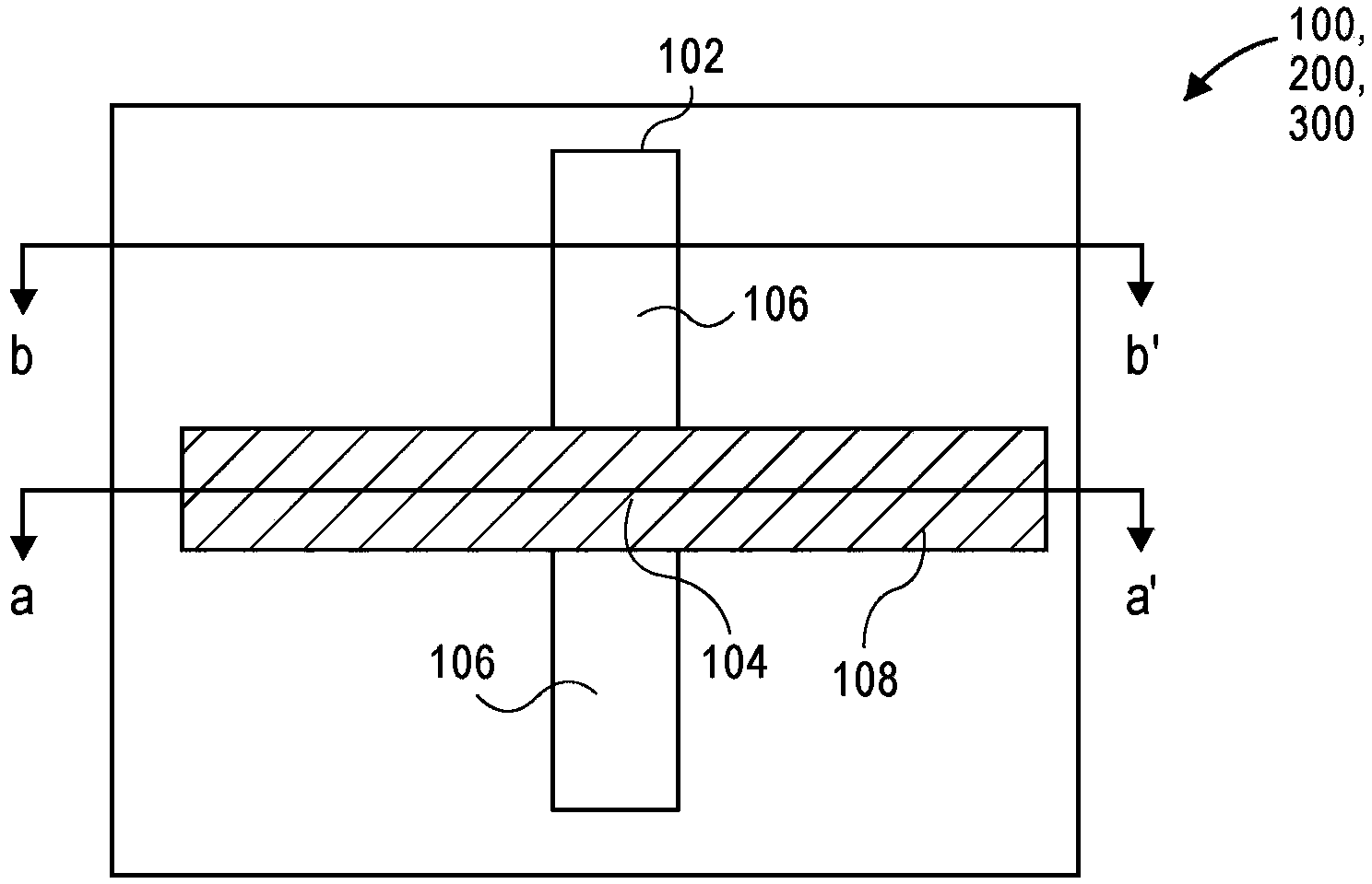
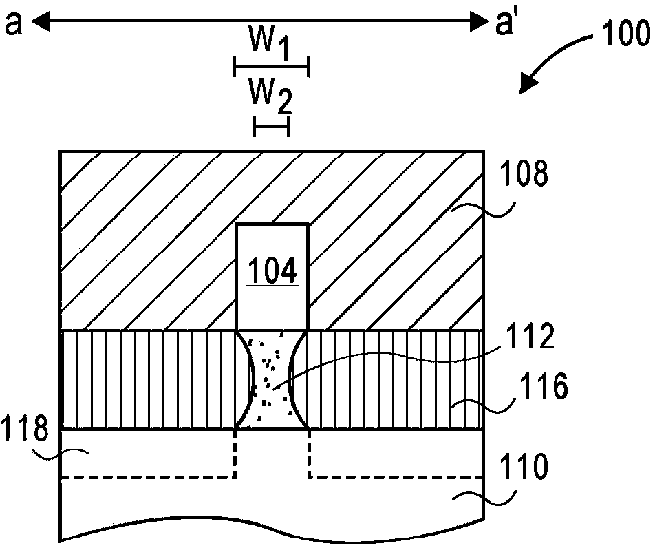
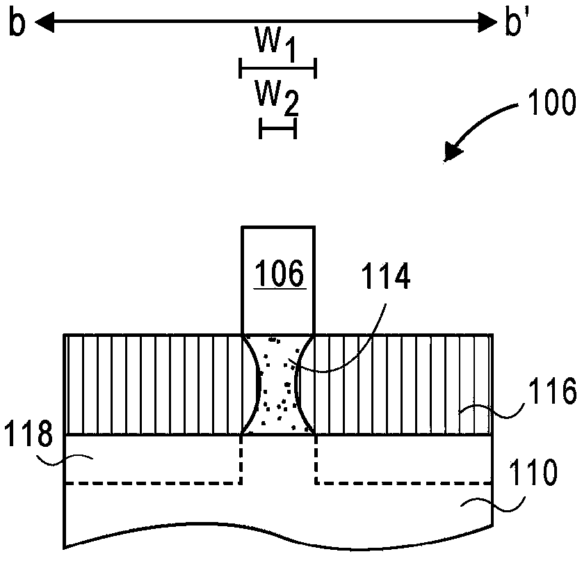
[0031] A semiconductor device having an isolated body portion is described. In the following description, numerous specific details are set forth, such as specific integration and material regimes, in order to provide a thorough understanding of embodiments of the invention. It will be apparent to those skilled in the art that embodiments of the invention may be practiced without these specific details. In other instances, well-known features, such as integrated circuit design layouts, have not been described in detail in order not to unnecessarily obscure the embodiments of the invention. Furthermore, it should be understood that the various embodiments shown in the drawings are illustrative representations and are not necessarily drawn to scale.

[0032] Methods of isolating a channel region or source and drain regions, or both, of a semiconductor body of a semiconductor device from an underlying semiconductor substrate, and the resulting structures are described. In an em...


PUM


Abstract

Semiconductor devices with isolated body portions are described. For example, a semiconductor structure includes a semiconductor body disposed above a semiconductor substrate. The semiconductor body includes a channel region and a pair of source and drain regions on either side of the channel region. An isolation pedestal is disposed between the semiconductor body and the semiconductor substrate. A gate electrode stack at least partially surrounds a portion of the channel region of the semiconductor body.

Description

technical field [0001] Embodiments of the invention are in the field of semiconductor devices, and in particular, in the field of semiconductor devices having isolated body portions. Background technique [0002] Over the past few decades, the scaling of features in integrated circuits has been the driving force behind the growing semiconductor industry. Scaling to smaller and smaller features enables increasing the density of functional units on the limited real estate of a semiconductor chip. For example, shrinking transistor size allows the number of memory devices included on a chip to increase, resulting in products with greater capacity. However, the quest for greater and greater capacity is not without its problems. The need to optimize the performance of each device has become increasingly apparent. [0003] In the fabrication of integrated circuit devices, multi-gate transistors, such as tri-gate transistors, have become more common as device dimensions continue ...

Claims


Application Information

Patent Timeline
Patent Type & Authority Applications(China)
IPC IPC(8): H01L29/78H01L21/336
CPCB82Y10/00H01L29/66795H01L29/775H01L29/0649H01L27/1203H01L29/0673H01L29/785H01L21/762H01L21/76216H01L29/7802H01L29/0653H01L29/42392H01L29/66818
Inventor A·卡佩拉尼S·M·塞亚T·加尼H·戈麦斯J·T·卡瓦列罗斯P·H·基斯S·金K·J·库恩A·D·利拉科R·里奥斯M·萨尼
Owner INTEL CORP
Why Eureka
Try Eureka