

Shift register and grid drive circuit
A shift register, source technology, applied in static memory, digital memory information, instruments, etc., can solve the problems of complicated circuit design and unfavorable development of narrow edge of display panel.
- Summary
- Abstract
- Description
- Claims
- Application Information
AI Technical Summary
Problems solved by technology
Method used
Image

Examples
Embodiment 1
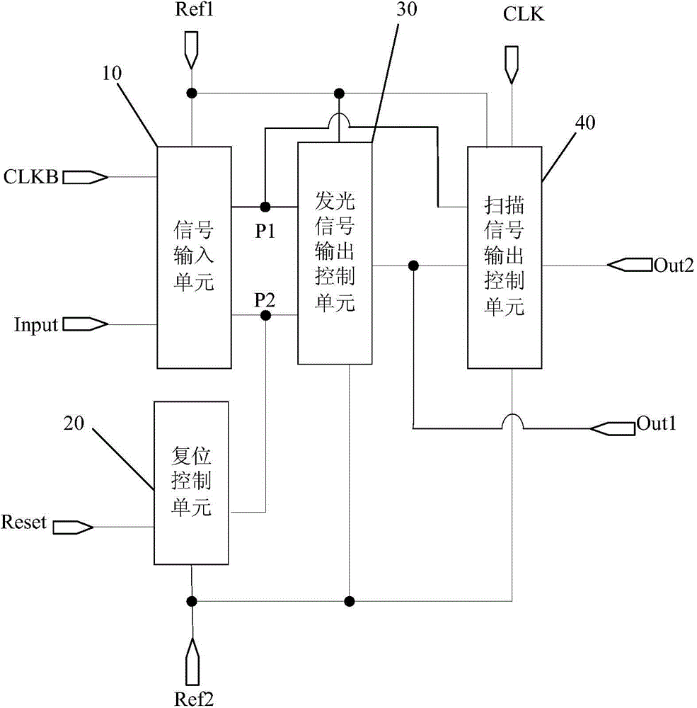
[0118] Example 1: Combining Figure 8a shown in the shift register as well as Figure 8b shown Figure 8a The input and output timing diagrams of the present invention describe the working process of the shift register provided by the embodiment of the present invention. Specifically, choose the Figure 8b There are four stages A to D in the input and output sequence diagram shown. In the following description, 1 represents a high-level signal, and 0 represents a low-level signal.
[0119]In phase A, Input=0, CLKB=0, CLK=1, Reset=1, Ref1=1. Because Reset=1, the ninth switch transistor T9 is turned off; because Input=0, the eighth switch transistor T8 is turned on, and Ref1 is turned on with the second node P2, so that the second node P2 is at a high level, thereby making the tenth switch transistor T8 turn on. The switch transistor T10 and the sixth switch transistor T6 are turned off, and the turned off sixth switch transistor T6 makes the first switch transistor T1 turn...
Embodiment 2
[0124] Embodiment 2: Combination Figure 9a shown in the shift register as well as Figure 9b shown Figure 9a The input and output timing diagrams of the present invention describe the working process of the shift register provided by the embodiment of the present invention. Specifically, choose the Figure 9b There are four stages A to D in the input and output sequence diagram shown. In the following description, 1 represents a high-level signal, and 0 represents a low-level signal.
[0125] In phase A, Input=1, CLKB=1, CLK=0, Reset=0, Ref1=0. Because Reset=0, the ninth switching transistor T9 is turned off; because Input=1, the eighth switching transistor T8 is turned on, and Ref1 is turned on with the second node P2, so that the second node P2 is at a low level, thereby making the tenth The switch transistor T10 and the sixth switch transistor T6 are turned off, and the closed sixth switch transistor T6 turns off the first switch transistor T1; at the same time, sinc...
PUM
 Abstract
Description
Claims
Application Information