Manufacturing method of gainp/gaas/ingaasp/ingaas four-junction cascaded solar cell

A technology of solar cells and manufacturing methods, which is applied to circuits, photovoltaic power generation, electrical components, etc., can solve problems such as increasing the difficulty of battery technology, achieve high photoelectric conversion efficiency, reduce production costs, and reduce consumption

Active Publication Date: 2017-01-25
SUZHOU INST OF NANO TECH & NANO BIONICS CHINESE ACEDEMY OF SCI
View PDF4 Cites 0 Cited by
  • Summary
  • Abstract
  • Description
  • Claims
  • Application Information

AI Technical Summary

Problems solved by technology

Therefore, it is necessary to obtain a thin layer of Ge before bonding, which will greatly increase the process difficulty of battery development.

Method used


Image

  • Manufacturing method of gainp/gaas/ingaasp/ingaas four-junction cascaded solar cell
  • Manufacturing method of gainp/gaas/ingaasp/ingaas four-junction cascaded solar cell
  • Manufacturing method of gainp/gaas/ingaasp/ingaas four-junction cascaded solar cell

Examples


Embodiment Construction

[0029] The technical solutions in the embodiments of the present invention will be described in detail below in conjunction with the accompanying drawings in the embodiments of the present invention. Obviously, the described embodiments are only some of the embodiments of the present invention, not all of them. Based on the embodiments of the present invention, all other embodiments obtained by persons of ordinary skill in the art without making creative efforts belong to the protection scope of the present invention.

[0030] The fabrication method of GaInP / GaAs / InGaAsP / InGaAs four-junction cascaded solar cells is as follows:

[0031] 1) Cell growth before bonding

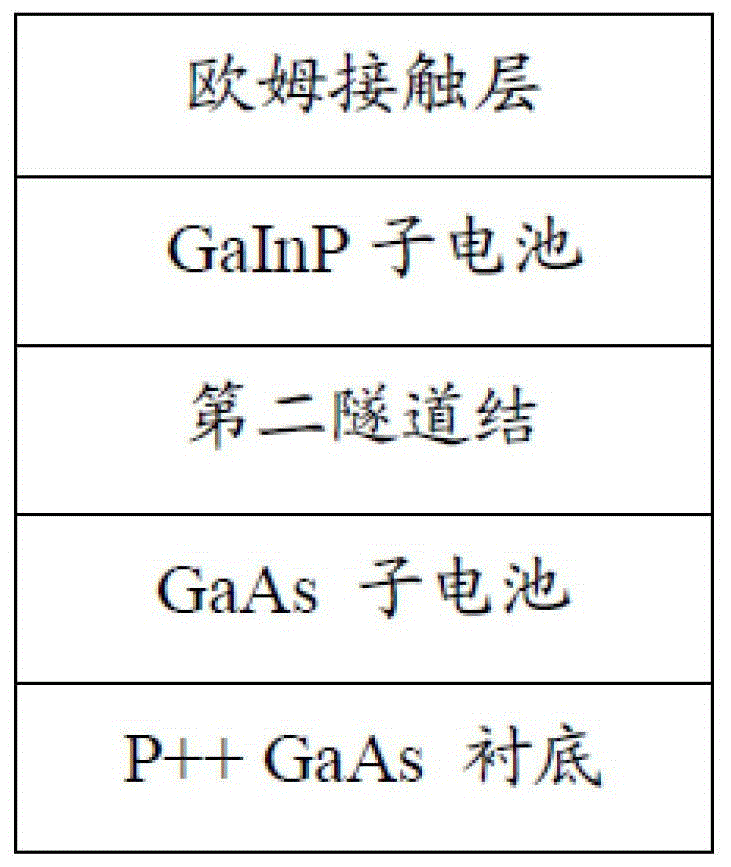
[0032] ginseng figure 1 As shown, a GaAs buffer layer of 0.2-1 μm is first grown on a GaAs substrate, and then a GaAs subcell, a second tunnel junction, a GaInP subcell, and a 500 nm GaAs contact layer are grown next.

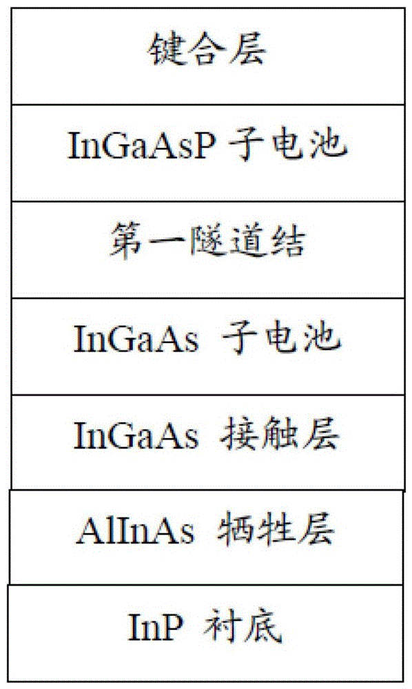
[0033] ginseng figure 2 As shown, a 0.2-1μm InP buffer layer is first grown on the InP substr...


PUM


Abstract

The invention discloses a method for manufacturing a GaInP / GaAs / InGaAsP / InGaAs four-junction cascading solar cell. Based on wafer bonding technology, integration of a GaAs substrate-based GaInP / GaAs double-junction solar cell and an InP substrate-based InGaAsP / InGaAs double-junction solar cell is realized. An InP substrate is stripped, GaAs is adopted as a supporting substrate, a four-junction solar cell with respective band gap energy of 1.89 / 1.42 / 1.05 / 0.72eV is realized, absorption and energy conversion of a full spectrum of sunlight are realized to a greater extent, and the stripped InP substrate can recycled after being polished, thereby reducing consumption of InP substrates. According to the four-junction solar cell provided by the invention, high cost caused by using a plurality of substrates in a mechanical laminate multi-junction solar cell system and optical loss caused by a complicated optical system in an optical integrated cell can be reduced, and the problem of lattice mismatch of material for growing a multi-junction cascading semiconductor solar cell is effectively solved. High voltage and low current output is realized, and resistance consumption in a high-power concentrator cell is reduced.

Description

technical field [0001] The invention belongs to the photovoltaic field, and in particular relates to a method for manufacturing a GaInP / GaAs / InGaAsP / InGaAs four-junction cascaded solar cell. Background technique [0002] Stimulated by the energy crisis triggered in the 1970s and driven by the demand for space vehicle energy systems, the field of photovoltaic technology has continuously made breakthroughs. Crystalline silicon solar cells, amorphous silicon solar cells, amorphous silicon thin-film solar cells, III-V compound semiconductor solar cells, II-VI compound semiconductor polycrystalline thin-film solar cells, etc. More and more solar cell technologies are maturing . The continuous improvement of photoelectric conversion efficiency and the continuous reduction of manufacturing costs have enabled photovoltaic technology to be widely used in space and on the ground. [0003] Looking back at the development of photovoltaic technology in the past 10 years, the multi-junc...

Claims


Application Information

Patent Timeline
Patent Type & Authority Patents(China)
IPC IPC(8): H01L31/18H01L31/0687H01L31/0693
CPCH01L31/078H01L31/1844Y02E10/544Y02P70/50
Inventor 赵勇明董建荣李奎龙孙玉润曾徐路于淑珍赵春雨杨辉
Owner SUZHOU INST OF NANO TECH & NANO BIONICS CHINESE ACEDEMY OF SCI
Why Eureka
Try Eureka