Array substrate, display panel and display device

An array substrate and matrix technology, which is applied in the display field, can solve the problems of uneven brightness of odd-numbered and even-numbered rows, skewed polarizers, horizontal stripes of liquid crystal display devices, etc., and achieves the effect of avoiding the horizontal stripe problem.

Active Publication Date: 2014-12-10
SHANGHAI AVIC OPTOELECTRONICS +1
View PDF10 Cites 15 Cited by
  • Summary
  • Abstract
  • Description
  • Claims
  • Application Information

AI Technical Summary

Problems solved by technology

In the process of making a liquid crystal display device, when the rubbing alignment direction deviates during rubbing or the polarizer is skewed when it is attached, uneven brightness between odd and even lines will appear during display, which will lead to liquid crystal display The device produces stripes

Method used


Image

  • Array substrate, display panel and display device
  • Array substrate, display panel and display device
  • Array substrate, display panel and display device

Examples


Embodiment 1

[0042] Based on the above description, Embodiment 1 of the present invention provides the following solution.

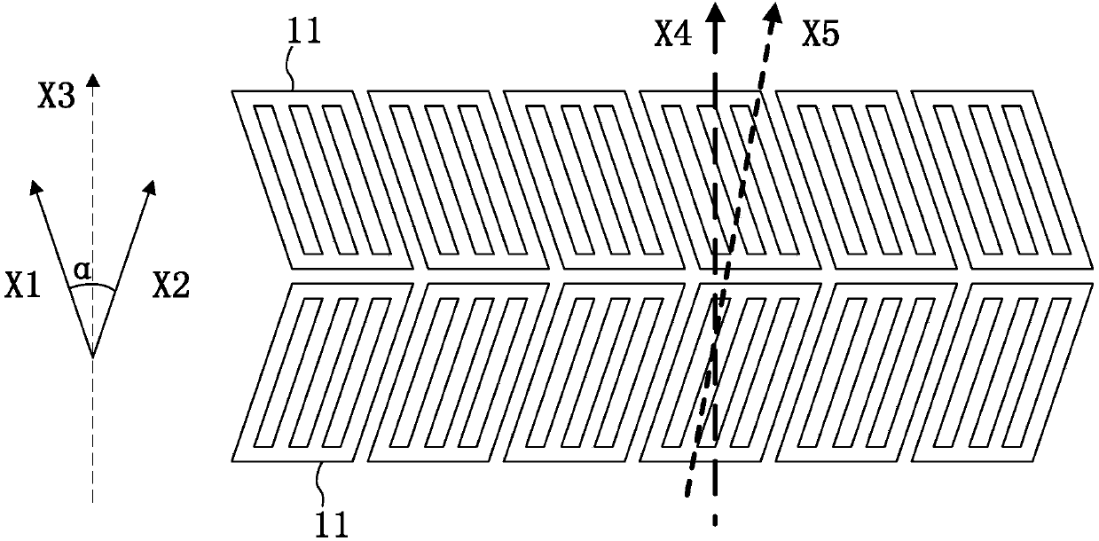
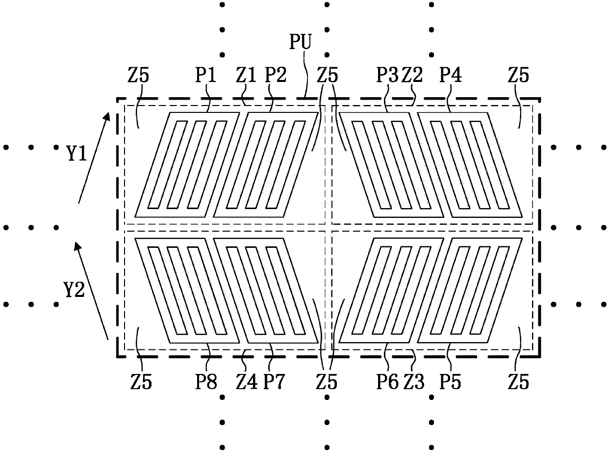
[0043] Embodiment 1 of the present invention provides an array substrate. Figure 1b It is a schematic structural diagram of an array substrate provided in Embodiment 1 of the present invention. see Figure 1b, the array substrate includes: a plurality of pixel units PU, the pixel unit PU includes a 2×2 sub-pixel region matrix, and the 2×2 sub-pixel region matrix includes a first sub-pixel region Z1, a second sub-pixel region arranged in sequence The pixel area Z2, the third sub-pixel area Z3 and the fourth sub-pixel area Z4; each of the sub-pixel areas includes at least two sub-pixel electrodes; each of the sub-pixel electrodes includes a strip electrode; the first sub-pixel In the pixel area Z1 and the third sub-pixel area Z3, at least one of the strip electrodes in the sub-pixel electrode is parallel to the first direction Y1; the second sub-pixel area Z2 and th...

Embodiment 2

[0054] exist Figure 1b In the pixel unit shown, the strip electrodes in all the sub-pixel electrodes in the first sub-pixel area Z1 and the third sub-pixel area Z3 are parallel to the first direction Y1, and the second sub-pixel area Z2 and the fourth sub-pixel area The strip electrodes in all the subpixel electrodes in Z4 are parallel to the second direction Y2, and the formed first region Z5 includes: the second subpixel electrode P2, the third subpixel electrode P3, the sixth subpixel electrode P6 and the seventh subpixel electrode P6. The first region Z5 formed by the sub-pixel electrode P7 and the first sub-pixel electrode P1, the fourth sub-pixel electrode P4, the fifth sub-pixel electrode P5 and the eighth sub-pixel electrode P8 are connected to the sub-pixel electrodes in the respective adjacent pixel units. The first zone Z5 is formed. Therefore, for each sub-pixel electrode, there is a first region Z5 corresponding thereto, so that a sub-pixel switch can be set in ...

Embodiment 3

[0058] On the basis of the structure of the array substrate described in Embodiment 1, the pixel unit on the array substrate of this embodiment may further be: the four sub-pixel regions respectively include three sub-pixel electrodes, and each of the four sub-pixel regions includes 1×3 sub-pixel electrode matrix; each of the first sub-pixel area and the third sub-pixel area has at least one sub-pixel electrode in which the strip electrodes are parallel to the first direction; the second The strip-shaped electrodes each having at least one sub-pixel electrode in the sub-pixel area and the fourth sub-pixel area are parallel to the second direction.

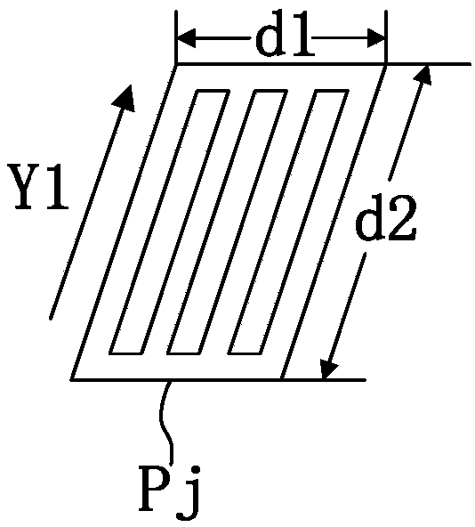
[0059] Figure 3a It is a schematic structural diagram of a pixel unit provided by Embodiment 3 of the present invention. see Figure 3a , in the pixel unit, each of the first sub-pixel area Z1 and the third sub-pixel area Z3 has a strip electrode in the sub-pixel electrode parallel to the first direction Y1; the second sub-pixel...


PUM


Abstract

The invention discloses an array substrate, a display panel and a display device. The array substrate comprises multiple pixel units with 2*2 sub-pixel region matrixes, and each sub-pixel region comprises two or more sub-pixel electrodes. A strip-shaped electrode in at least one sub-pixel electrode in the first sub-pixel region and a strip-shaped electrode in at least one sub-pixel electrode in the third sub-pixel region are in parallel with the first direction, and a strip-shaped electrode in at least one sub-pixel electrode in the second sub-pixel region and a strip-shaped electrode in at least one sub-pixel electrode in the fourth sub-pixel region are in parallel with the second direction. The first direction and the second direction are intersected, the sub-pixel electrodes where the strip-shaped electrodes in parallel with the first direction are located and the sub-pixel electrodes where the strip-shaped electrodes in parallel with the second direction are located define a first region, and a sub-pixel switch is arranged in the first region. According to the technical scheme, under the condition that the friction alignment direction deviates, or a polarizer deflects, the transverse striation problem can be effectively avoided.

Description

technical field [0001] The present invention relates to the field of display technology, in particular to an array substrate, a display panel and a display device. Background technique [0002] Liquid crystal display devices have the advantages of thinness, low power consumption and low radiation, and are widely used in various fields. With the development of liquid crystal display technology, the display effect of liquid crystal display devices has been continuously improved. [0003] In the prior art liquid crystal display device, the strip electrodes in each row of pixel electrodes on the array substrate adopt a pseudo-double-domain structure arrangement, that is, for the strip electrodes in any two adjacent rows of pixel electrodes, one row The parallel direction of the strip-shaped electrodes is different from that of the other row of strip-shaped electrodes. In the process of making a liquid crystal display device, when the rubbing alignment direction deviates during...

Claims


Application Information

Patent Timeline
Patent Type & Authority Applications(China)
IPC IPC(8): G02F1/1343
CPCG02F1/134336G02F1/13439G02F1/134345H01L27/124H01L29/40H01L29/786
Inventor 金慧俊李岩松王苗苗徐鑫邵琬童
Owner SHANGHAI AVIC OPTOELECTRONICS
Why Eureka
Try Eureka