Image capture lens, image capture device, and portable terminal

A camera lens and lens technology, applied in optical components, instruments, optics, etc., can solve problems such as difficulty in achieving high performance, performance degradation, and increase in elements, and achieve good telecentric characteristics and ensure the effect of back focal length.

Inactive Publication Date: 2014-12-10
KONICA MINOLTA INC
View PDF8 Cites 0 Cited by
  • Summary
  • Abstract
  • Description
  • Claims
  • Application Information

AI Technical Summary

Problems solved by technology

However, since the three-element structure has more elements than the two-element structure, the performance degradation due to the accumulation of individual

Method used


Image

  • Image capture lens, image capture device, and portable terminal
  • Image capture lens, image capture device, and portable terminal
  • Image capture lens, image capture device, and portable terminal

Examples


Embodiment 1

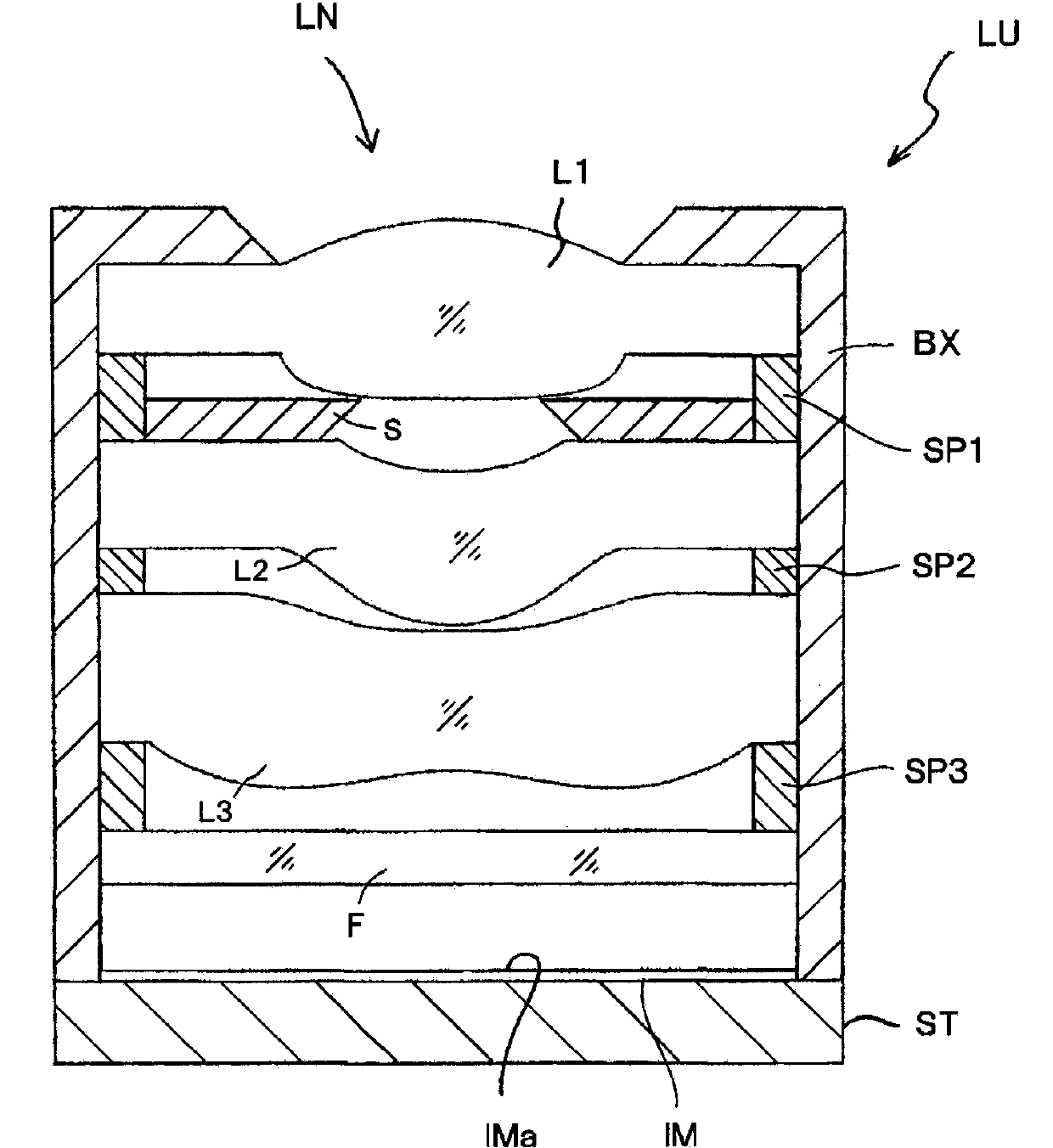
[0147] Table 1 shows lens data in Example 1. Figure 4 It is a sectional view of the lens of Example 1. The imaging lens of Embodiment 1 includes a first lens L1, an aperture stop S, a second lens L2, and a third lens L3 in sequence from the object side. The first lens L1 is a positive lens with a convex surface on the side of the object, and the second lens L2 is a convex lens on the object side. The third lens L3 is a positive meniscus lens with a concave surface, and the third lens L3 is a negative lens with an aspheric surface that is concave near the optical axis and has an inflection point within the effective diameter, and convex around the lens. CG is a parallel plate in which a cover glass or an IR cut filter is assumed, and IM is an imaging surface of a solid-state imaging element.

[0148] [Table 1]

[0149] [Example 1]

[0150] Reference wavelength = 587.56nm

[0151] Unit: mm

[0152]

[0153] Aspheric coefficient

[0154]

[0155]

[0156]

[01...

Embodiment 2

[0159] Table 2 shows lens data in Example 2. Figure 6 It is a sectional view of the lens of Example 2. The imaging lens of Embodiment 2 includes a first lens L1, an aperture stop S, a second lens L2, and a third lens L3 in sequence from the object side. The first lens L1 is a positive lens with a convex surface on the side of the object, and the second lens L2 is a convex lens on the object side. The third lens L3 is a positive meniscus lens with a concave surface, and the third lens L3 is a negative lens with an aspheric surface that is concave near the optical axis and has an inflection point within the effective diameter, and convex around the lens. CG is a parallel plate in which a cover glass or an IR cut filter is assumed, and IM is an imaging surface of a solid-state imaging element.

[0160] [Table 2]

[0161] [Example 2]

[0162] Reference wavelength = 587.56nm

[0163] Unit: mm

[0164]

[0165]

[0166] Aspheric coefficient

[0167]

[0168]

[0169...

Embodiment 3

[0172] Table 3 shows lens data in Example 3. Figure 8 It is a sectional view of the lens of Example 3. The imaging lens of Embodiment 3 includes a first lens L1, an aperture stop S, a second lens L2, and a third lens L3 in order from the object side. The first lens L1 is a positive lens with a convex surface on the side of the object, and the second lens L2 is a convex lens on the object side. The third lens L3 is a positive meniscus lens with a concave surface, and the third lens L3 is a negative lens with an aspheric surface that is concave near the optical axis and has an inflection point within the effective diameter, and convex around the lens. CG is a parallel plate in which a cover glass or an IR cut filter is assumed, and IM is an imaging surface of a solid-state imaging element.

[0173] [table 3]

[0174] [Example 3]

[0175] Reference wavelength = 587.56nm

[0176] Unit: mm

[0177]

[0178]

[0179] Aspheric coefficient

[0180]

[0181]

[0182]...


PUM


Abstract

Provided are an image capture lens with a three-layer configuration with which, in a bright lens which has an angle of field of 65° or more and an F/stop of 3 or less, while having lower error sensitivity and better moldability, etc., than conventional types, all aberrations are corrected, as well as an image capture device and a portable terminal which employs same. An image capture lens is formed from, in order from the objective side, a first lens, an aperture iris, a second lens, and a third lens. The first lens is a positive lens with a convex objective-side face, the second lens is a positive meniscus lens with a concave objective-side face, and the third lens is a negative lens with an objective-side face which is concave near the optical axis, an inflection point within an effective radius, and an aspherical convex face near the periphery of the lens, whereby the following formulae are satisfied: -5.0 < r3/f < -0.4 (1), and 0.0 < f1/f2 < 5.0 (2), wherein r3 is the radius of curvature in mm of the second lens objective-side face, f is the focal length in mm of the total assembly, f1 is the focal length in mm of the first lens, and f2 is the focal length in mm of the second lens.

Description

technical field [0001] The present invention relates to an imaging lens suitable for an imaging device using a solid-state imaging element such as a CCD (Charge Coupled Device: Charge Coupled Device) image sensor, a CMOS (Complementary Metal Oxide Semiconductor: Complementary Metal Oxide Semiconductor) image sensor, and the like. An imaging device and a portable terminal using an imaging lens. Background technique [0002] In recent years, with the improvement in performance and miniaturization of imaging elements using solid-state imaging elements such as CCD (Charge Coupled Device) image sensors and CMOS (Complementary Metal Oxide Semiconductor) image sensors, mobile phones equipped with imaging devices have become popular. , Portable information terminal. In addition, there is an increasing demand for further miniaturization and higher performance of imaging lenses mounted on these imaging devices. Recently, two types of high-resolution and high-performance main cameras...

Claims


Application Information

Patent Timeline
IPC IPC(8): G02B13/00G02B13/18
CPCG02B13/0035
Inventor 川崎贵志
Owner KONICA MINOLTA INC
Why Eureka
Try Eureka