Touch displaying device and substrate

A technology of touch display substrate and display stage, applied in the direction of instruments, nonlinear optics, optics, etc., can solve the problems affecting the arrangement of liquid crystal molecules, light leakage, etc., achieve the effect of solving light leakage and poor screen display effect, and improving the display effect

Active Publication Date: 2014-12-24
SHANGHAI TIANMA MICRO ELECTRONICS CO LTD +1
View PDF6 Cites 37 Cited by
  • Summary
  • Abstract
  • Description
  • Claims
  • Application Information

AI Technical Summary

Problems solved by technology

[0003] In view of this, the present invention provides a touch display device and a touch display substrate to solve the problem of light leakage caused by voltage fluctuations on data lines or scan lines affecting the arrangement of liquid crystal molecules in the prior art

Method used


Image

  • Touch displaying device and substrate
  • Touch displaying device and substrate
  • Touch displaying device and substrate

Examples


Embodiment 1

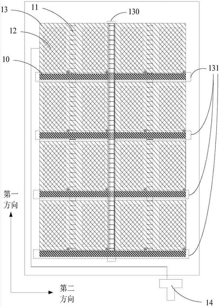
[0032] This embodiment provides a touch display substrate, such as figure 2 and Figure 3a As shown, it includes a plurality of data lines 20, a plurality of gate lines 21 that insulate and intersect with the data lines 20, a plurality of pixel electrodes 22 and a plurality of common electrodes 23, and there are slits between two adjacent common electrodes 23 (not shown), wherein the pixel electrode 22 is located in the area surrounded by the data line 20 and the gate line 21, and the projection of the common electrode 23 on the touch display substrate covers at least one pixel electrode 22 on the touch display substrate projection, that is, the projection of one common electrode 23 can cover the projection of one pixel electrode 22, and can also cover the projection of two pixel electrodes 22; and the shielding electrode (not shown) is located above the slit, In the display phase, a common voltage is applied to the shielding electrodes; wherein, the shielding electrodes inc...

Embodiment 2

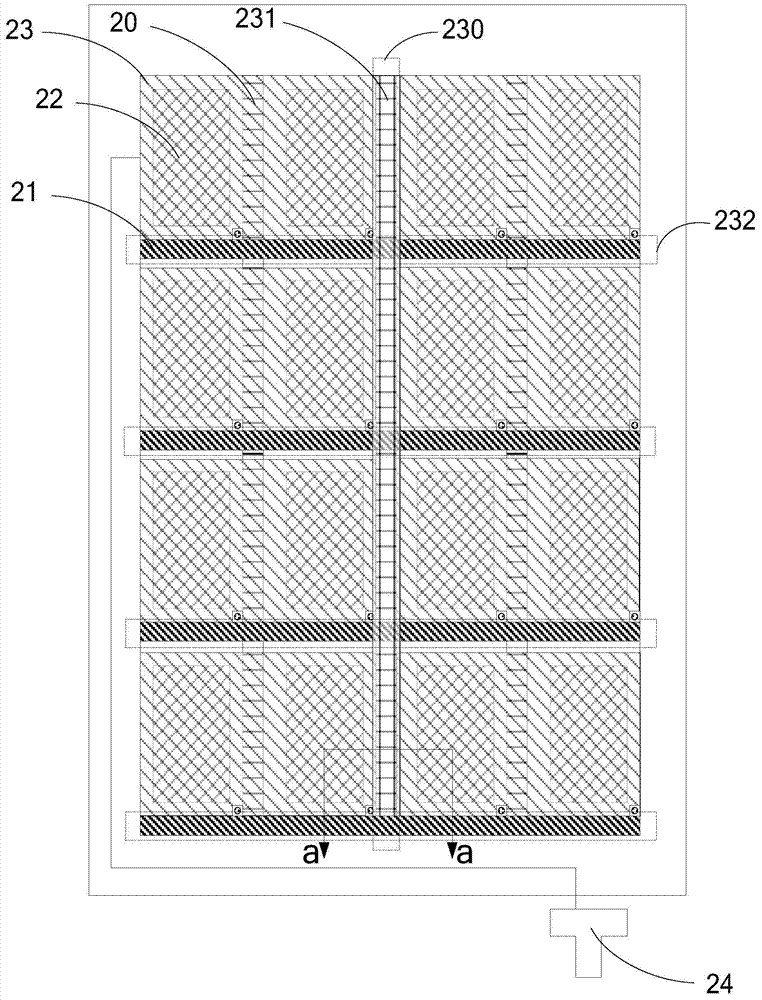
[0052] This embodiment provides a touch display substrate, and the structure of the touch display substrate provided in Embodiment 2 is substantially the same as that provided in Embodiment 1, as shown in Figure 5 and Figure 6a As shown, including the data line 20, the gate line 21, the pixel electrode 22, the common electrode 23, the first direction slit 230 and the second direction slit 231, the difference between the second embodiment and the first embodiment is that this embodiment In Example 2, a second shielding electrode 233 is further included above the slit 232 in the second direction. The second shielding electrode 233 is preferably a metal electrode for shielding the voltage fluctuation on the gate line 21 at the slit 232 in the second direction. Solve the problems of light leakage and poor picture display effect caused by the voltage fluctuation on the gate line.

[0053] In this embodiment, the projection of the slit 232 in the second direction on the touch dis...

Embodiment 3

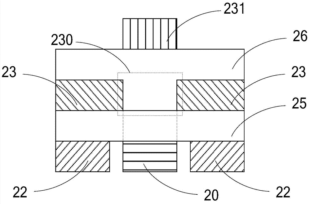
[0069] This embodiment provides a touch display substrate, such as Figure 8 , Figure 3a and Figure 6a As shown, the touch display substrate includes a data line 20, a gate line 21, a pixel electrode 22, a common electrode 23, a first direction slit 230 and a first shielding electrode 231, a second direction slit 232 and a second shielding electrode 233.

[0070] Further, the first shielding electrode 231 may include a plurality of sub-first shielding electrodes 2310 and a first fracture 2311 between two adjacent sub-first shielding electrodes 2310, and the second shielding electrode 231 may include a plurality of sub-second shielding electrodes 2330 As well as the second break 2330 located between two adjacent sub-second shielding electrodes 2330, the structure and function of the first shielding electrode in this embodiment are the same as the structure and function of the first shielding electrode in Embodiment 1, the sub-second shielding electrode The structure and fu...


PUM


Abstract

The invention provides a touch displaying device and substrate. A plurality of data lines, a plurality of gate lines, a plurality of pixel electrodes, a plurality of common electrodes and covering electrodes are included. The gate lines and the data lines are in insulation crossing. In the extending direction of the gate lines and/or the data lines, a carving seam is formed between two adjacent common electrodes. The covering electrodes are placed above the carving seams. At a displaying stage, common voltage is applied to the covering electrodes. The projection of the carving seams on the touch displaying substrate and the projection of the data lines and/or the gate lines on the touch displaying substrate comprise coinciding parts. The projection of the covering electrodes on the touch displaying substrate at least covers the data lines and/or the gate lines of the coinciding parts. Accordingly, voltage fluctuation on the data lines and/or scanning lines can be screened through the covering electrodes, and the problems of light leakage and poor image displaying effect caused by voltage fluctuation are solved.

Description

technical field [0001] The present invention relates to the field of display technology, and more specifically, to a touch display device and a touch display substrate. Background technique [0002] Today, touch display devices are becoming more and more popular. However, in actual use, it is found that there is light leakage in the touch display device, which affects the display effect of the picture. Contents of the invention [0003] In view of this, the present invention provides a touch display device and a touch display substrate to solve the problem in the prior art that the arrangement of liquid crystal molecules is affected by voltage fluctuations on data lines or scan lines, resulting in light leakage. [0004] To achieve the above object, the present invention provides the following technical solutions: [0005] The invention provides a touch display substrate, comprising: [0006] A plurality of data lines; a plurality of gate lines insulated and intersected ...

Claims


Application Information

Patent Timeline
Patent Type & Authority Applications(China)
IPC IPC(8): G02F1/1362G02F1/1343G02F1/1333
Inventor 王丽花杜凌霄姚绮君吴天一
Owner SHANGHAI TIANMA MICRO ELECTRONICS CO LTD
Why Eureka
Try Eureka