Multilayer circuit board and manufacturing method thereof

A technology of multilayer circuit board and manufacturing method, which is applied in the direction of multilayer circuit manufacturing, printed circuit manufacturing, printed circuit, etc., can solve the problems of unfavorable process simplification, high production cost, and many pressing times, so as to save raw materials, Improved yield rate and easy repair

Inactive Publication Date: 2014-12-24
AVARY HLDG (SHENZHEN) CO LTD +1
View PDF7 Cites 19 Cited by
  • Summary
  • Abstract
  • Description
  • Claims
  • Application Information

AI Technical Summary

Problems solved by technology

When using the layer-up method to make multi-layer circuit boards, if a circuit board with more layers is made, the number of pressing times will be correspondingly more, which is not conducive to the simplification of the process, the production cost is relatively high, and the production efficiency is relatively low. Low

Method used


Image

  • Multilayer circuit board and manufacturing method thereof
  • Multilayer circuit board and manufacturing method thereof
  • Multilayer circuit board and manufacturing method thereof

Examples


Embodiment Construction

[0020] The multi-layer circuit board and the manufacturing method thereof provided by the technical solution will be further described in detail below with reference to the accompanying drawings and embodiments.

[0021] The manufacturing method of the multilayer circuit board provided by the embodiment of this technical solution includes the following steps:

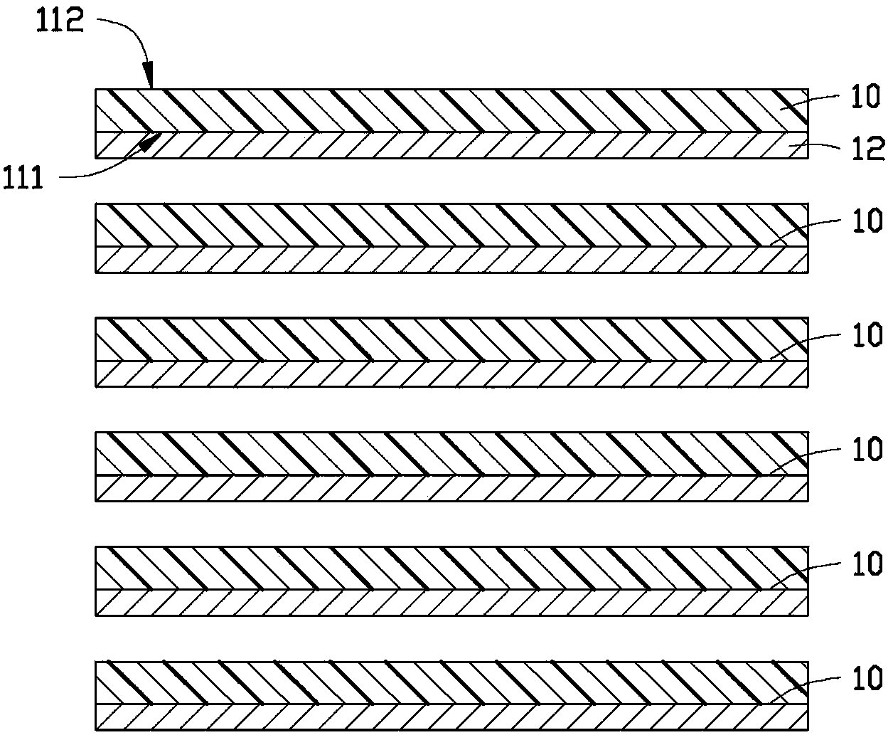
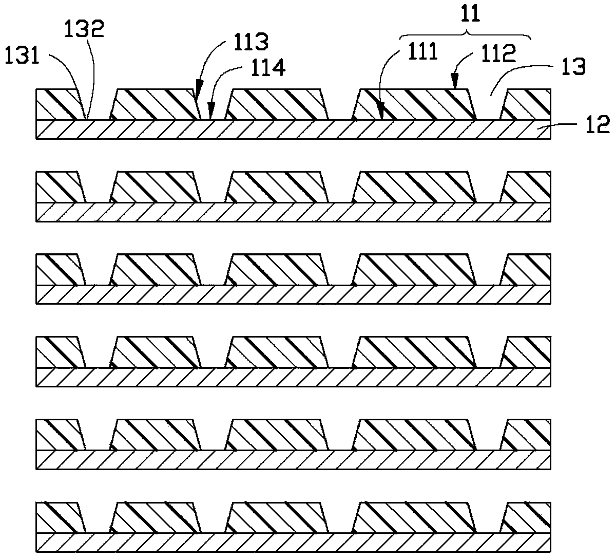
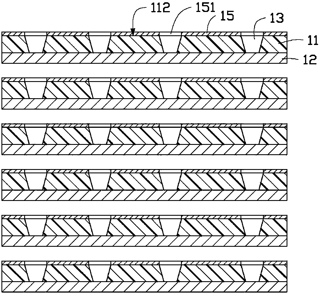
[0022] As a first step, see figure 1 , and N copper clad substrates 10 are provided. Among them, N is a natural number greater than or equal to 3. Each copper clad substrate 10 includes an insulating layer 11 and a copper foil layer 12 bonded to one side of the insulating layer 11 .

[0023] The insulating layer 11 includes a first surface 111 adhering to the copper foil layer 12 and a second surface 112 opposite to the first surface 111 . The insulating layer 11 is a thermoplastic resin, preferably a thermotropic liquid crystal polymer (LCP) with low water absorption, low thermal expansion coefficient, high heat res...


PUM

PropertyMeasurementUnit
heightaaaaaaaaaa

Abstract

A multilayer circuit board comprises N conducting circuit graphs, two of the conducting circuit graphs are located on the two outermost sides of the multilayer circuit board respectively, and an insulating layer is arranged between every two adjacent conducting circuit graphs for separation and is made of thermoplastic resin. At least one blind hole is formed between every two adjacent conducting circuit graphs and comprises a side wall and a bottom wall. Conducting layers are formed on the surface of the side wall and the surface of the bottom wall of each blind hole, an electroplate filling material is arranged on the surface of each conducting layer, and each blind hole is filled with the corresponding electroplate filling material; each blind hole comprises a bottom end close to the bottom wall and an opening end opposite to the bottom end. The electroplate filling materials protrude out of the conducting layers at the opening ends, and every two adjacent conducting circuit graphs are electrically connected through the corresponding conducting layer and the corresponding electroplate filling material. The invention further provides a manufacturing method of the multilayer circuit board.

Description

technical field [0001] The invention relates to a circuit board manufacturing technology, in particular to a multi-layer circuit board and a manufacturing method thereof. Background technique [0002] With the development of electronic products in the direction of miniaturization and high speed, circuit boards have also developed from single-sided circuit boards and double-sided circuit boards to multi-layer circuit boards. Multilayer circuit board refers to a circuit board with multiple layers of conductive lines, which has more wiring area and higher interconnection density, so it is widely used, see the literature Takahashi, A. Ooki, N. Nagai, A. Akahoshi , H. Mukoh, A. Wajima, M. Res. Lab., High density multilayer printed circuit board for HITAC M-880, IEEE Trans. on Components, Packaging, and Manufacturing Technology, 1992, 15(4): 418-425 . At present, multi-layer circuit boards are usually fabricated by a build-up method, that is, the multi-layer circuit boards are f...

Claims


Application Information

Patent Timeline
Patent Type & Authority Applications(China)
IPC IPC(8): H05K3/46H05K1/02
CPCH05K3/421H05K3/4617H05K3/4632H05K2201/0129H05K2201/0141H05K2201/096Y10T156/1056
Inventor 李育贤钟福伟刘瑞武
Owner AVARY HLDG (SHENZHEN) CO LTD
Why Eureka
Try Eureka