Array substrate, driving method thereof, display panel, and display device

An array substrate and gate driving technology, applied in the fields of array substrate and its driving method, display panel and display device, can solve the problems of high temperature of integrated circuits, high production cost, complicated process, etc., and achieve lower power consumption and lower power consumption. The effect of power consumption

Active Publication Date: 2017-12-26
BOE TECH GRP CO LTD +1
View PDF10 Cites 0 Cited by
  • Summary
  • Abstract
  • Description
  • Claims
  • Application Information

AI Technical Summary

Problems solved by technology

Since this structure needs to manufacture TFTs on both sides of a row of pixel electrodes, the manufacturing cost is relatively large and the process is relatively complicated in the actual manufacturing process.
[0005] For the double-gate structure, in order to reduce the power consumption of the source drive integrated circuit, that is, the positive and negative polarity of the signal input by the Data line does not change, adopt image 3 The pixel structure shown, when the Gate line is used figure 1 and figure 2 In the progressive scanning method, the polarities of two adjacent pixel units in the same row are the same, that is, the pixels in the dot flip realized in this case are flipped by two adjacent pixel points, which cannot be realized as figure 1 and figure 2 dot flip in
[0006] To sum up, in the prior art, when the signal input through the Data line is continuously switched between positive and negative polarities to achieve point inversion, it will cause excessive power consumption of the source driver integrated circuit, resulting in an increase in the temperature of the internal integrated circuit. ; When dot flipping is realized through the structure of the new array substrate, the production cost is higher and the process is more complicated

Method used


Image

  • Array substrate, driving method thereof, display panel, and display device
  • Array substrate, driving method thereof, display panel, and display device
  • Array substrate, driving method thereof, display panel, and display device

Examples


Embodiment Construction

[0048] Embodiments of the present invention provide an array substrate and a driving method thereof, a display panel, and a display device, which are used to reduce the power consumption of a source driving integrated circuit when realizing point inversion.

[0049] The array substrate and the driving method thereof provided by specific embodiments of the present invention will be described in detail below with reference to the accompanying drawings.

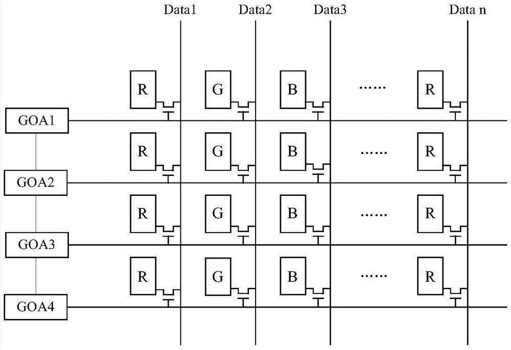
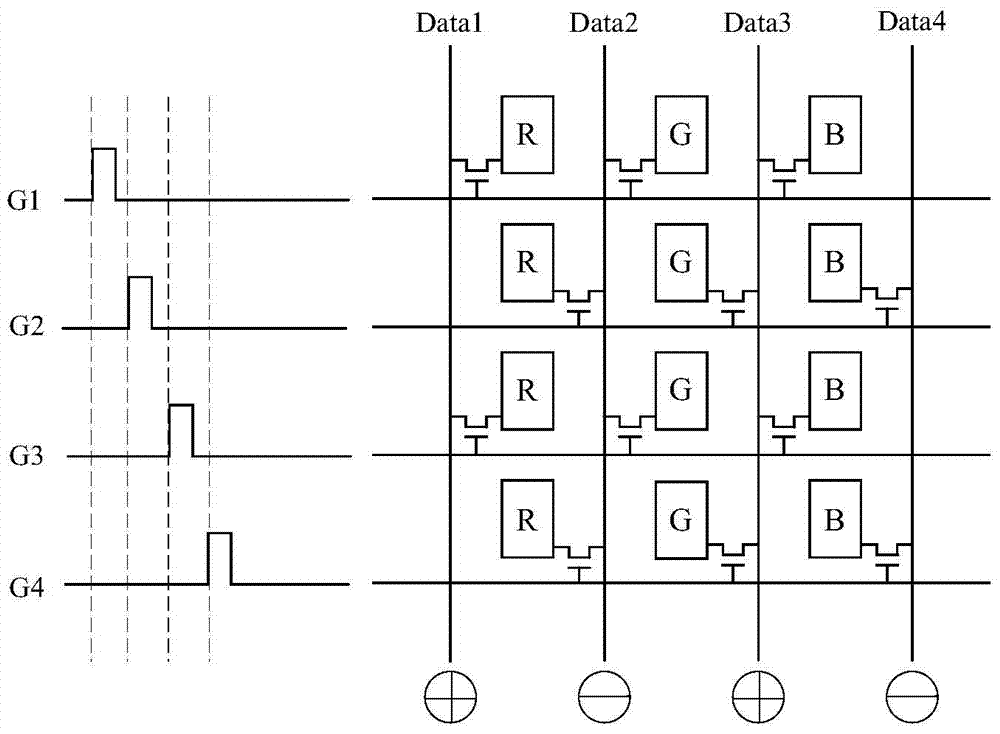
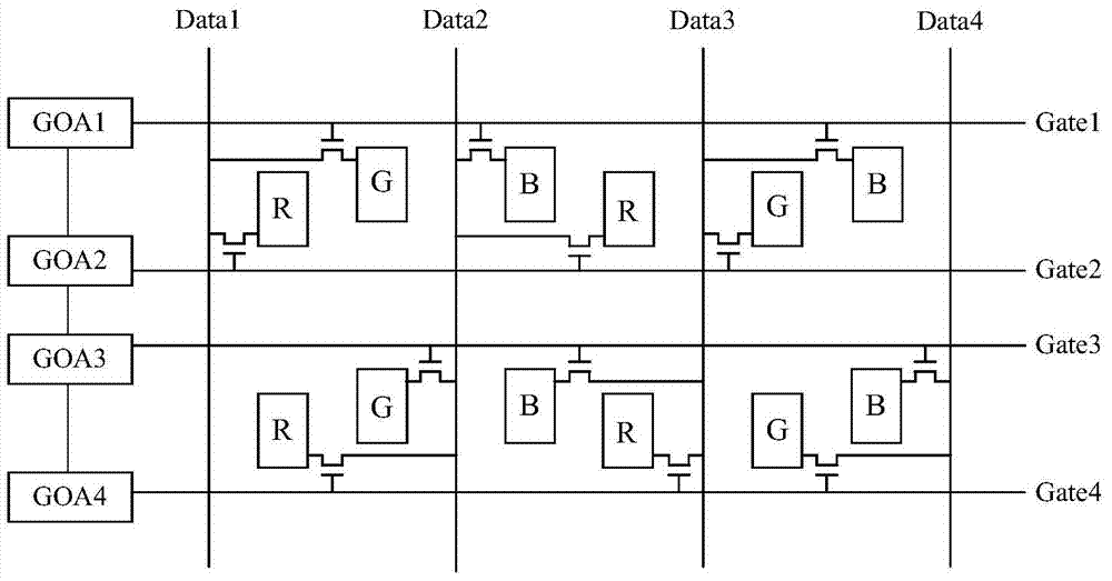
[0050] like Figure 4 As shown, a specific embodiment of the present invention provides an array substrate, which includes a plurality of pixel units 40 arranged in an array, a plurality of data lines connected to the source driver integrated circuit, such as Data1, Data2, Data3, Datan, and a gate electrode. Multiple gate lines connected by the drive circuit, such as Gate1, Gate2, Gate3 and Gate4,

[0051] Each odd-numbered row of gate lines is correspondingly connected to a gate driving sub-circuit. For example, the gate line ...


PUM


Abstract

The invention discloses an array substrate, a driving method thereof, a display panel and a display device, which are used for reducing power consumption of a source driving integrated circuit when realizing dot inversion. All gate drive sub-circuits connected to odd-numbered gate lines in the array substrate are connected in cascade to form the first gate drive circuit; all gate drive sub-circuits connected to even-numbered gate lines are connected in cascade to form the second gate drive circuit. Gate drive circuit; within half a display period of one frame of image display, the gate lines of odd rows receive the gate drive signal output by the first gate drive circuit, and each data line receives the first gate drive signal output by the source drive integrated circuit. Source drive signal; in the other half of the display period of one frame of image display, the gate lines of the even rows receive the gate drive signal output by the second gate drive circuit, and each data line receives the first gate drive signal output by the source drive integrated circuit. Two source driving signals; the polarity of the first source driving signal is opposite to that of the second source driving signal.

Description

technical field [0001] The present invention relates to the technical field of displays, and in particular, to an array substrate and a driving method thereof, a display panel and a display device. Background technique [0002] The prior art liquid crystal display (Liquid Crystal Display, LCD) includes an array substrate on which a plurality of thin film transistors (Thin Film Transistor, TFT) are distributed, the drain electrode of one TFT on the array substrate is connected to a pixel electrode correspondingly, and the TFT The source electrode of the TFT is correspondingly connected to a data (Data) line, and the gate electrode of the TFT is correspondingly connected to a gate (Gate) line. The Gate Driver On Array (GOA) technology of the array substrate integrates the thin film transistor as the gate switch circuit on the array substrate, thereby omitting the gate driver integrated circuit. In the array substrate, each row of Gate lines is correspondingly connected to a G...

Claims


Application Information

Patent Timeline
Patent Type & Authority Patents(China)
IPC IPC(8): G02F1/1362G02F1/133G09G3/36
Inventor 高玉杰李承珉朴相镇
Owner BOE TECH GRP CO LTD
Why Eureka
Try Eureka