Array substrate, manufacturing method thereof, and display device

The technology of an array substrate and its manufacturing method is applied in the field of the array substrate and its manufacturing method and display device, and can solve the problems of low aperture ratio and transmittance of the display panel, unsatisfactory picture quality and low resolution of the display panel, and achieve Effects of improving image quality, increasing aperture ratio and transmittance, and increasing resolution

Active Publication Date: 2016-05-25
BOE TECH GRP CO LTD +1
View PDF5 Cites 0 Cited by
  • Summary
  • Abstract
  • Description
  • Claims
  • Application Information

AI Technical Summary

Problems solved by technology

[0005] However, the array substrate manufactured in this way has the following disadvantages: first, there are many black matrix light-shielding areas corresponding to the grid structure composed of data scanning lines and gate scanning lines, and the aperture ratio and transmittance of the display panel are relatively low; The resolution of the panel is limited by the data scanning line and the gate scanning line, which is not conducive to the design and manufacture of high PPI (Pixelsperinch, pixels per inch) products; the three driving methods are line inversion mode, and the picture quality is not ideal

Method used


Image

  • Array substrate, manufacturing method thereof, and display device
  • Array substrate, manufacturing method thereof, and display device
  • Array substrate, manufacturing method thereof, and display device

Examples


Embodiment Construction

[0035] Embodiments of the present invention will be described in detail below with reference to the accompanying drawings.

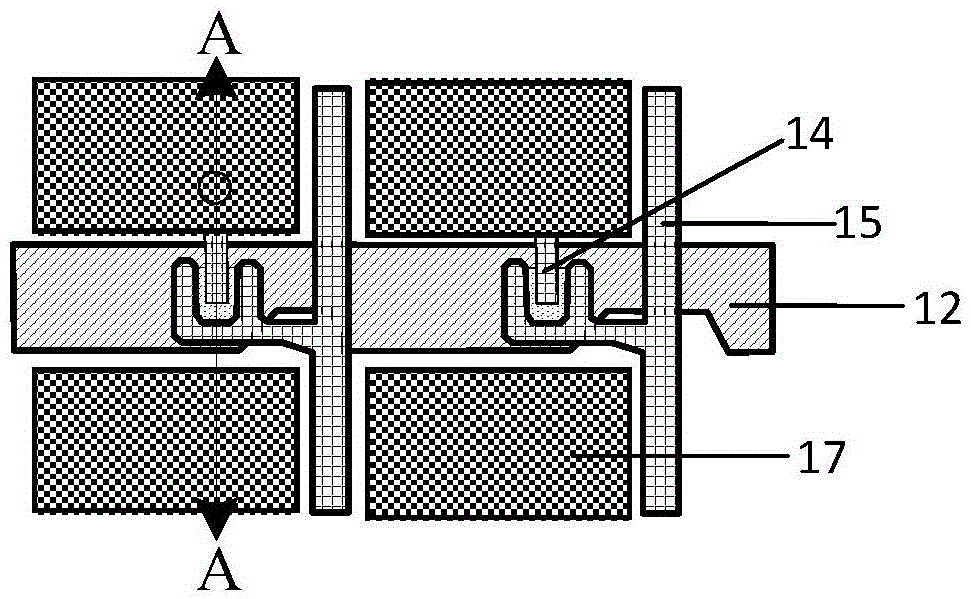
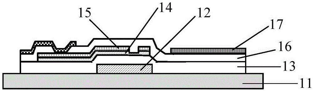
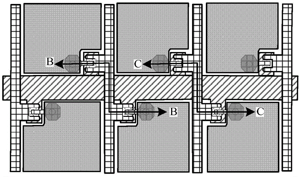
[0036] Figure 3 to Figure 5 A schematic diagram showing the structure of an array substrate according to an embodiment of the present invention, wherein image 3 shows a top view of an array substrate structure according to an embodiment of the present invention, Figure 4 shows along the image 3 The cross-sectional view of the B-B line intercepted, Figure 5 shows along the image 3 The cross-sectional view taken along line C-C of . From Figure 3 to Figure 5 It can be seen from the figure that the array substrate structure according to the embodiment of the present invention has two layers of gate scanning lines stacked up and down, which are the first gate scanning line 2 and the second gate scanning line 8 respectively. The intervals are separated by the first gate insulating layer 3, and the second gate insulating layer 9 is formed on the se...


PUM


Abstract

The present invention relates to an array substrate, a manufacturing method thereof, and a display device. The array substrate includes: a substrate, a first grid scanning line formed on the substrate, and a first gate scanning line formed on the first grid scanning line. A gate insulating layer, an active layer formed on the first gate insulating layer, a data scanning line formed on the active layer and perpendicular to the first gate scanning line, and a data scanning line formed on the first gate insulating layer The pixel electrode in the pixel unit defined by the first gate scan line and the data scan line on the data scan line, the array substrate further includes: a second gate scan line formed on the first gate scan line above or below a gate scan line, the second gate scan line substantially coincides with the first gate scan line in the stacking direction of the array substrate, and the second gate scan line coincides with the The first gate scan line, the active layer, the data scan line and the pixel electrode are insulated.

Description

technical field [0001] The present invention relates to the field of display technology, in particular, to an array substrate, a manufacturing method thereof, and a display device. Background technique [0002] With the development of display technology, display panels with high transmittance, large size, low power consumption and low cost have become the future development direction. [0003] The gate scanning lines of the existing TFT-LCD array substrates are mostly single-line structures. figure 1 shows a top view of an existing array substrate structure, figure 2 shows along the figure 1 A cross-sectional view taken along line A-A. Such as figure 1 and 2 As shown, a gate scanning line 12 is formed on a glass substrate 11, and an insulating layer 13 is covered on the gate scanning line 12, and the insulating layer 13 is usually made of silicon nitride. An active layer 14 is formed on the insulating layer 13, and a data scanning line 15 is formed on the active layer...

Claims


Application Information

Patent Timeline
Patent Type & Authority Patents(China)
IPC IPC(8): G02F1/1362G02F1/1333
CPCG02F1/1362G02F1/136209G09G3/3659H01L27/1237H01L27/124H01L27/1259
Inventor 吴洪江袁剑峰
Owner BOE TECH GRP CO LTD
Why Eureka
Try Eureka