

Fixing board for PCB (Printed Circuit Board) and machining method thereof
A technology for PCB boards and fixed boards, applied in printed circuit parts, electrical components, printed circuit manufacturing, etc., to achieve the effects of reducing processing time, compact product structure, and simplifying changes
- Summary
- Abstract
- Description
- Claims
- Application Information
AI Technical Summary
Problems solved by technology
Method used
Image

Examples
Embodiment Construction
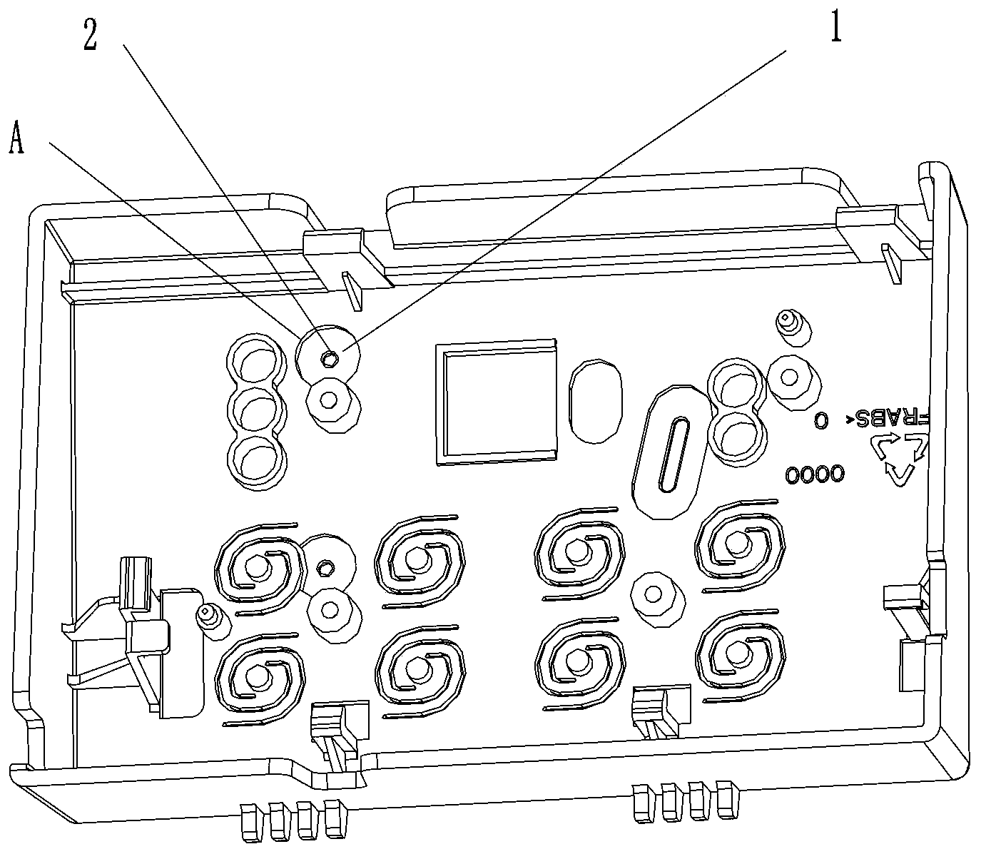
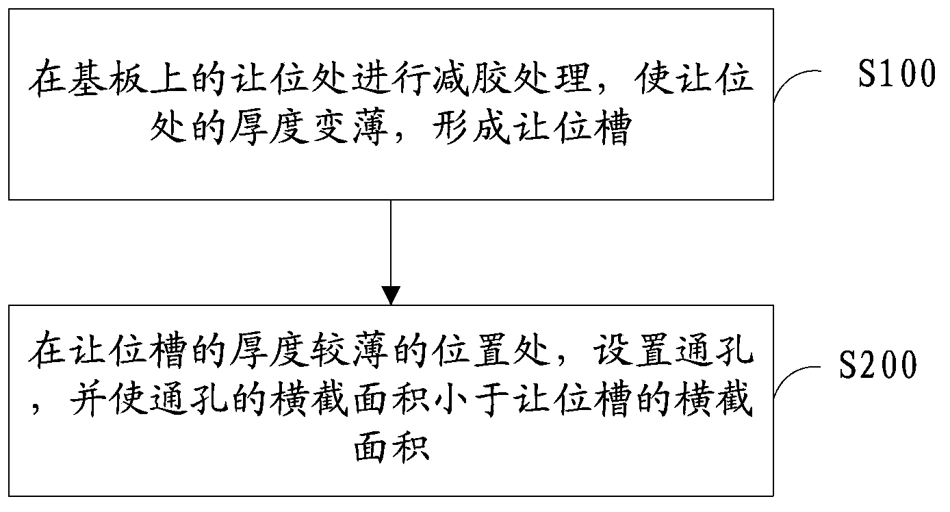
[0021] The embodiment of the present invention provides a kind of fixing plate of PCB board, such as figure 2 As shown, including the base plate, also includes the relief slot 1;
[0022] There are multiple relief grooves 1, which are respectively arranged at multiple relief positions of the substrate;
[0023] The step-off groove 1 is a groove that matches the appearance of the electrical components on the PCB that need to make way, and is used to accommodate the electrical components that need to make way on the PCB;
[0024] The bottom of the relief groove 1 is provided with a through hole 2 , and the cross-sectional area of the through hole 2 is smaller than that of the relief groove 1 .
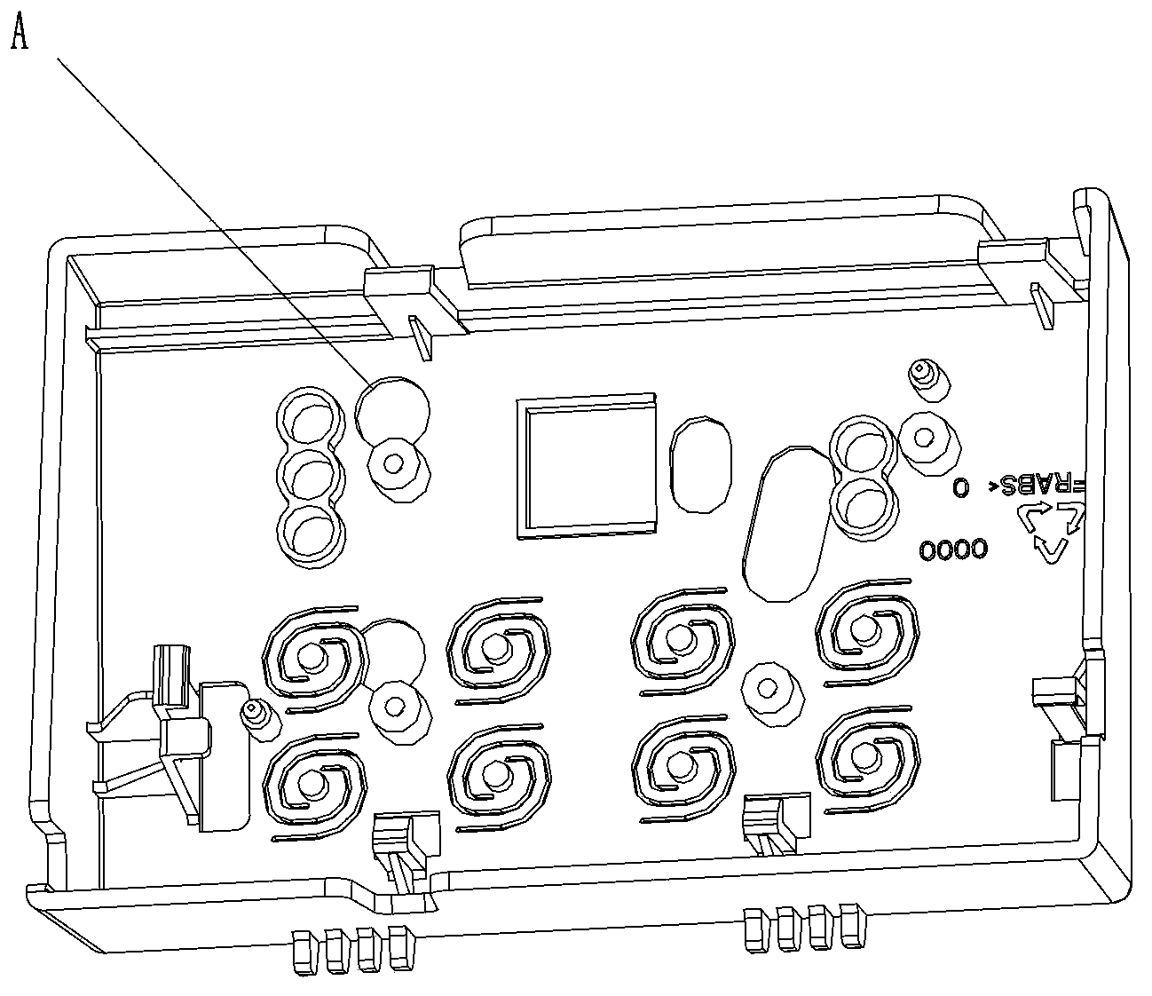
[0025] The place where the substrate needs to make way, that is, the A region shown in the figure, and the make way groove 1 is arranged in the A region.
[0026] Preferably, as a possible implementation manner, the depth of the relief groove 1 is equal to the distance that the elec...
PUM
 Abstract
Description
Claims
Application Information