
Local high-precision printed circuit board and manufacturing method thereof

A printed circuit board, high-precision technology, used in printed circuits, printed circuit manufacturing, printed circuit components, etc., can solve the problem of difficult to meet the drilling requirements of high-end printed circuit boards, insufficient drilling accuracy control, and scrapped boards. and other problems, to achieve the effect of improving the drilling alignment accuracy, reducing the scrap rate, and being easy to control.

Active Publication Date: 2015-01-07
GUANGZHOU FASTPRINT CIRCUIT TECH +2
View PDF6 Cites 26 Cited by
  • Summary
  • Abstract
  • Description
  • Claims
  • Application Information

AI Technical Summary

Problems solved by technology

Although this method can solve the drilling of most printed circuit boards, it is difficult to meet the drilling requirements of high-end printed circuit boards, such as printed circuit boards with extremely high local precision requirements and boards with large differences in expansion and contraction in different regions. Parts, etc., if the drilling positioning method is adopted, it will easily lead to insufficient control of the drilling accuracy in the local high-precision area, resulting in internal short, resulting in the scrapping of the board

Method used


Image

  • Local high-precision printed circuit board and manufacturing method thereof
  • Local high-precision printed circuit board and manufacturing method thereof
  • Local high-precision printed circuit board and manufacturing method thereof

Examples


Embodiment

[0032] This embodiment is a method for preparing a local high-precision printed circuit board. The entire printed circuit board is divided into a high-precision pattern area and a common pattern area. The number of layers of the printed circuit board is 24. The distance from the hole to the conductor in the precision pattern area is 3.5 mils.

[0033] The preparation method includes the following steps: inner layer pattern making, pressing, drilling, outer layer dry film and post-processes;

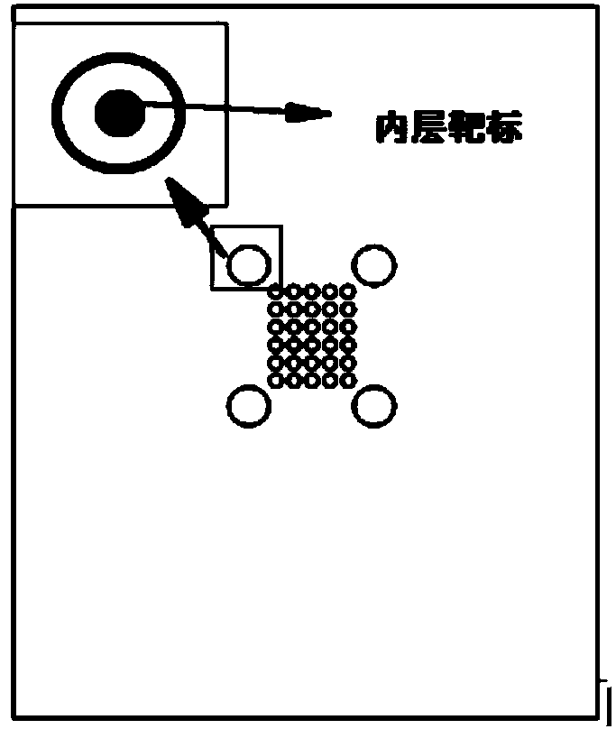
[0034] In the step of making the inner layer graphics, 4 positioning targets (such as figure 1 Shown);

[0035] In the pressing step, the Pin-Lam process is used for production;

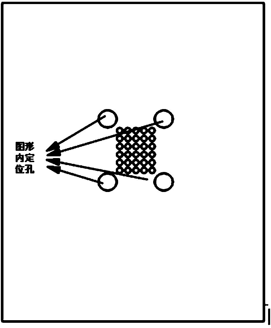
[0036] After pressing, use the inner layer positioning target of the graphic to determine the positioning hole in the graphic, and then use the X-RAY target punching machine to punch out the positioning hole in the graphic (such as figure 2 As shown), the positioning holes in the graph are non-metallized holes with a d...


PUM

PropertyMeasurementUnit
Apertureaaaaaaaaaa

Abstract

The invention discloses a local high-precision printed circuit board and a manufacturing method thereof. The whole printed circuit board is divided into a high-precision graphic area and a common graphic area. The manufacturing method comprises the steps of inner-layer graph manufacturing, press-fitting, drilling, outer-layer film drying and follow-up procedures. According to the press-fitting step, the Pin-Lam technology is adopted for conducting manufacturing; after the press-fitting step is executed, a graphic inner positioning hole is punched, so that a local expansion coefficient of the high-precision graphic area is calculated. According to the drilling step, a local drilling file is set according to the local expansion coefficient, meanwhile, an LDI datum hole is formed, drilling is carried out on the high-precision graphic area, and the datum hole is drilled; then drilling is carried out on the common graphic area through the whole board expansion coefficient. According to the outer-layer film drying step, the LDI technology is adopted. According to the manufacturing method, the drilling alignment precision of the local high-precision printed circuit board can be effectively improved, highly-difficult drilling can be carried out, the drilling misregistration scrap rate is greatly reduced, and the process is simple.

Description

Technical field [0001] The invention relates to the field of printed circuit board manufacturing, in particular to a local high-precision printed circuit board and a preparation method thereof. Background technique [0002] With the continuous development of electronic products in the direction of multi-function, small size, light weight, and high performance, the requirements for the miniaturization and high density of printed circuit boards (PCB) are also increasing. The drilling of the board is reflected in the small hole diameter (mechanical drilling 0.1mm), high density, high accuracy (the distance between the hole and the conductor is less than or equal to 5mil when the number of layers is greater than or equal to 6). [0003] The existing drilling positioning method and the processing method of the drill belt are as follows: the positioning hole is punched by the central reference method, and then the whole plate is drilled through a coefficient of expansion and contraction....

Claims


Application Information

Patent Timeline
IPC IPC(8): H05K1/11H05K3/40
CPCH05K1/116H05K3/40H05K2203/0221H05K2203/15
Inventor 袁处赵新乔书晓
Owner GUANGZHOU FASTPRINT CIRCUIT TECH
Learn More