A LED miniaturized power supply

A technology of power supply and power management, applied in the field of power supply, can solve the problems of large heat generation, unstable output, and rising heat generation of IC chips, and achieve the effects of stable power supply performance, cost reduction, and long service life.

Active Publication Date: 2017-12-15
常州优派斯电气科技有限公司
View PDF11 Cites 0 Cited by
  • Summary
  • Abstract
  • Description
  • Claims
  • Application Information

AI Technical Summary

Problems solved by technology

[0002] The current LED power supply methods mainly include the following types: one is resistance-capacitance step-down, which is formed by pasting and inserting resistance-capacity components on the aluminum substrate, with low power factor (about 0.4-0.5) and low power utilization rate (below 70%). The current output is unstable with the fluctuation of the grid voltage, and cannot pass conduction, radiation and other certifications; the second is the switching power supply, which is made of complex electronic components such as integrated ICs and coils. It is bulky and cannot be directly placed in E14, E12 and other lamp holders; The cost is high, which is 2-8 times that of the product of the present invention; the third is the ordinary linear constant current scheme, the linear constant current IC wafer is packaged into chips according to the ordinary IC packaging process, and the chips and simple electronic components are welded on the aluminum substrate, and the input In the case of power grid voltage fluctuations, the output is unstable like the resistance-capacitance power supply scheme, and the IC chip generates a lot of heat, especially when the load voltage and input voltage are large. great deviation
The above-mentioned several kinds of power supplies are either bulky and costly, and in the light bulb product that meets one of the application applications of the present invention in structure, the cost can not meet the demand of mass consumption; big inconvenience

Method used


Image

  • A LED miniaturized power supply
  • A LED miniaturized power supply
  • A LED miniaturized power supply

Examples


Embodiment Construction

[0021] The present invention will be further described below in conjunction with accompanying drawing of description:

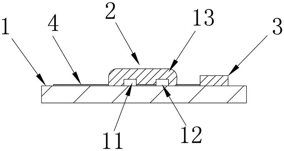
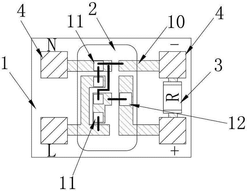
[0022] as attached Figure 1~2 As shown, the present invention discloses a LED miniaturized power supply, comprising a ceramic PCB substrate 1 and a silver paste circuit 10 sintered on the ceramic PCB substrate 1, the ceramic PCB substrate 1 is provided with a power management IC module 2, and the power supply In the management IC module, there are wafers with linear constant current function and auxiliary function devices directly packaged on the ceramic PCB substrate 1, and electronic components 3 are arranged on the periphery of the power management IC module 2, and the power management IC module 2 Input and output pads 4 are provided on both sides of the ceramic PCB substrate 1, silver paste lines are sintered on the ceramic PCB substrate 1, and the power management IC module 2 includes a wafer 11, an auxiliary function device 12 and a wafer 11 covered T...


PUM


Abstract

The invention discloses an LED miniature power supply which comprises a ceramic PCB substrate and a silver paste circuit sintered on the ceramic PCB substrate. A power supply management IC module is disposed on the ceramic PCB substrate. An electronic component is disposed on the periphery of the power supply management IC module. Input-output bonding pads are disposed on two sides of the power supply management IC module. The power supply management IC module comprises a wafer, an auxiliary functional device and an insulating point rubber layer. The LED miniature power supply has the advantages that the power supply is super small in size, capable of being placed in lamp heads such as E12, stable in performance and high in cost performance, the power supply can be matched with various dimmers on market to achieve dimming, the power supply can pass safety, transmission and radiation authentication, the power factor of the power supply is larger than 0.85, the utilization rate of the power supply is larger than 90%, the power supply has an overvoltage and overpower intelligent protection function, and the like.

Description

technical field [0001] The invention relates to a power supply, in particular to a miniaturized LED power supply. Background technique [0002] The current LED power supply methods mainly include the following types: one is resistance-capacitance step-down, which is formed by pasting and inserting resistance-capacity components on the aluminum substrate, with low power factor (about 0.4-0.5) and low power utilization rate (below 70%). The current output is unstable with the fluctuation of the grid voltage, and cannot pass conduction, radiation and other certifications; the second is the switching power supply, which is made of complex electronic components such as integrated ICs and coils. It is bulky and cannot be directly placed in E14, E12 and other lamp holders; The cost is high, which is 2-8 times that of the product of the present invention; the third is the ordinary linear constant current scheme, the linear constant current IC wafer is packaged into chips according t...

Claims


Application Information

Patent Timeline
Patent Type & Authority Patents(China)
IPC IPC(8): F21V23/00F21Y115/10
CPCH05B47/00
Inventor 贺能
Owner 常州优派斯电气科技有限公司
Why Eureka
Try Eureka