Electrophoretic apparatus, manufacturing method of electrophoretic apparatus, and electronic apparatus
A technology of an electrophoresis device and a manufacturing method, which can be applied in the directions of instruments, nonlinear optics, optics, etc., can solve the problems such as the deterioration of the display quality of electrophoretic particles
- Summary
- Abstract
- Description
- Claims
- Application Information
AI Technical Summary
Problems solved by technology
Method used
Image
Examples
no. 1 Embodiment approach
[0088]
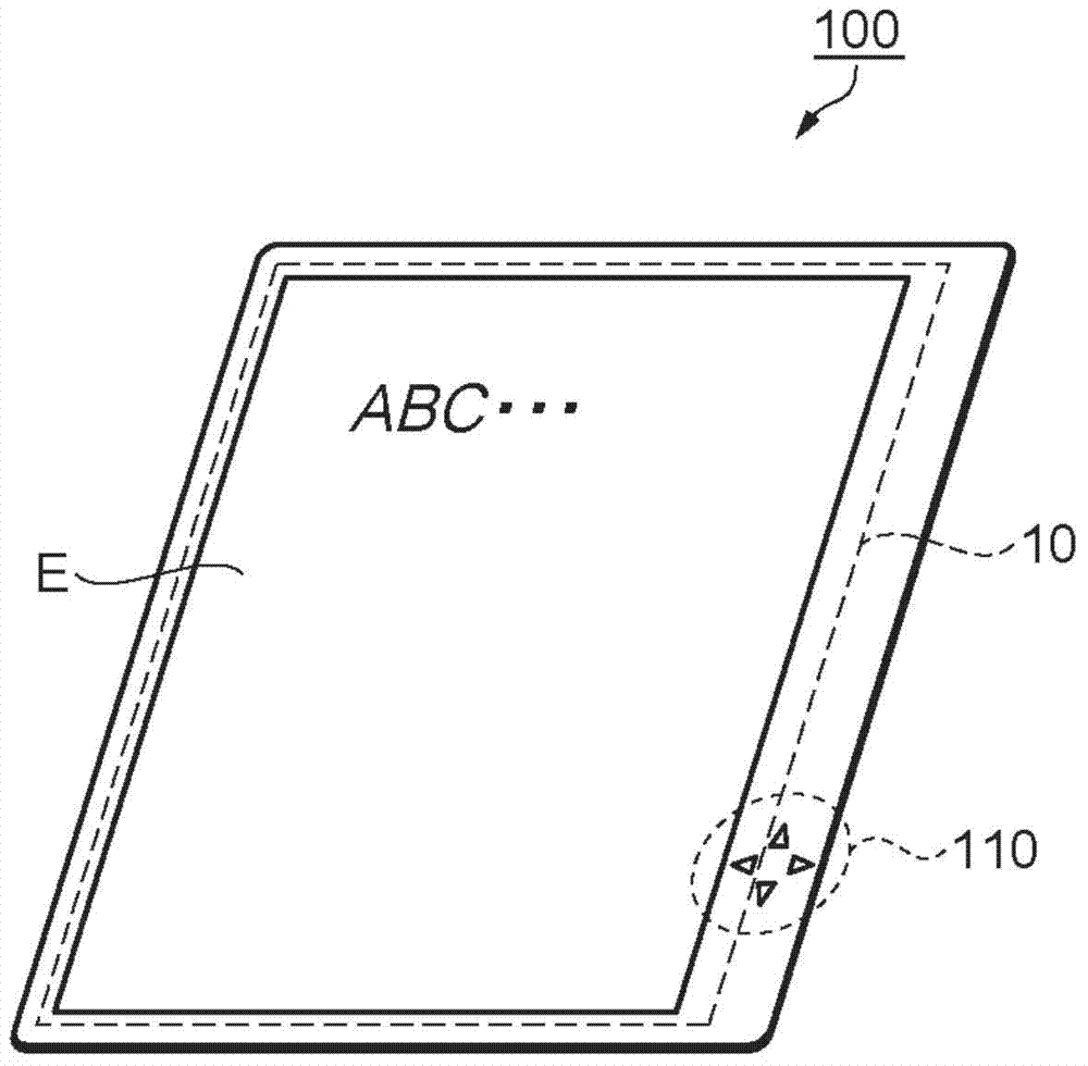
[0089] figure 1 It is a perspective view of an electronic device equipped with an electrophoretic device. As follows, while referring to figure 1 The structure of the electronic device will be described.
[0090] Such as figure 1 As shown, the electronic device 100 includes the electrophoretic device 10 and an interface for operating the electronic device 100 . The so-called interface is specifically the operation unit 110 and includes switches and the like.
[0091] The electrophoretic device 10 is a display module having a display area E. As shown in FIG. The display area E includes a plurality of pixels, and an image is displayed on the display area E by electrically controlling these pixels.
[0092] In addition, the electronic device 100 including the electrophoretic device 10 can also be applied to electronic paper (EPD: Electronic Paper Display), watches, wearable devices, and the like.
[0093]
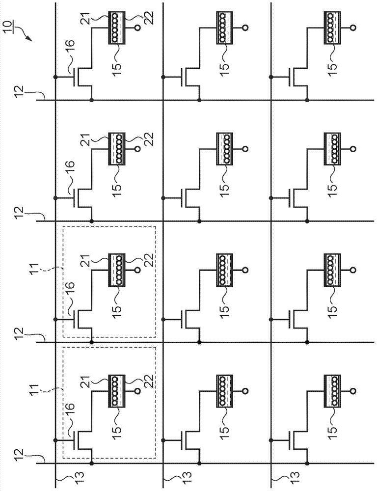
[0094] figure 2 is an equivalent circuit diagram sho...
no. 2 Embodiment approach
[0165]
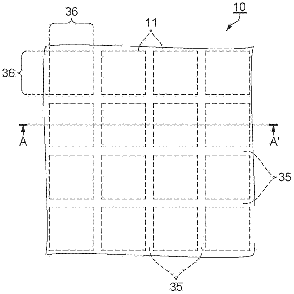
[0166] Figure 14 It is a schematic plan view showing the structure of the electrophoretic device. Figure 15 is along Figure 14 A schematic cross-sectional view of the line A-A' of the electrophoretic device shown. As follows, while referring to Figure 14 as well as Figure 15 The structure of the electrophoresis device will be described.
[0167] Such as Figure 14 as well as Figure 15 As shown, the electrophoretic device 210 has an element substrate 251 as a first substrate, a counter substrate 252 as a second substrate, and an electrophoretic layer 233 . A pixel electrode 221 is arranged for each pixel 211 on the first base material 231 including, for example, a light-transmitting glass substrate constituting the element substrate 251 .
[0168] If described in detail, as Figure 14 as well as Figure 15 As shown, the pixels 211 (pixel electrodes 221 ) are formed, for example, in a matrix when viewed from above. As a material of the pixel electrode ...
Deformed example 1
[0233] Instead of arranging the first sealing member 14a and the second sealing member 14b as the sealing portion 14 as in the above-mentioned first embodiment, as long as it has a sufficient sealing function, only the first sealing member 14a may be arranged. , and only the second sealing member 14b may be arranged. In addition, instead of arranging two seals, the first seal 214a and the second seal 214b, as the seal portion 214 as in the above-mentioned second embodiment, as long as it has a sufficient sealing function, it is also possible to arrange only As for the first seal 214a, only the second seal 214b may be arranged.
PUM
| Property | Measurement | Unit |
|---|---|---|
| elastic modulus | aaaaa | aaaaa |
| elastic modulus | aaaaa | aaaaa |
| thickness | aaaaa | aaaaa |
Abstract
Description
Claims
Application Information


