Liquid crystal display
A liquid crystal display, liquid crystal layer technology, applied in static indicators, instruments, nonlinear optics, etc., can solve the problems of color purity decline, cross-talk, display quality decline, etc., to achieve the display quality decline Wide viewing angle characteristics, prevent alignment Disturbance, effect of preventing crosstalk phenomenon
- Summary
- Abstract
- Description
- Claims
- Application Information
AI Technical Summary
Problems solved by technology
Method used
Image
Examples
no. 1 Embodiment
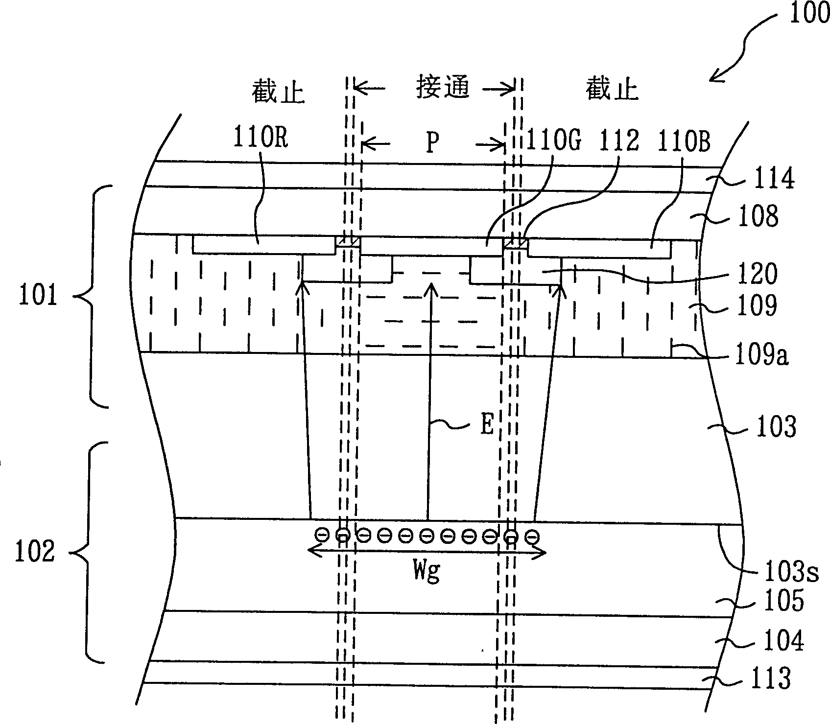
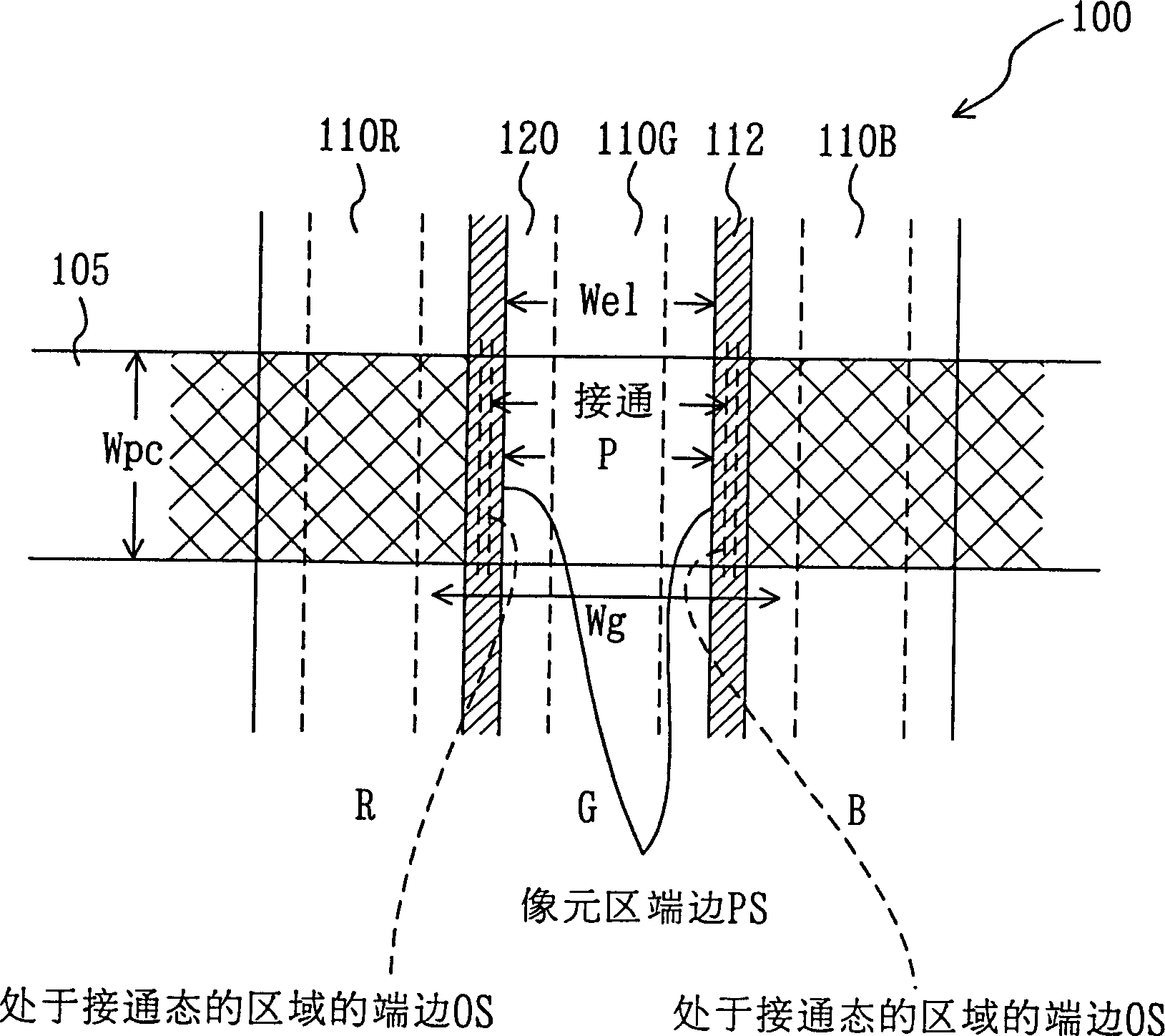
[0143] The plasma addressed liquid crystal display 100 in the first embodiment is shown in Figure 1A and Figure 1B middle. Like the conventional plasma-addressable liquid crystal display 200 described above, the plasma-addressable liquid crystal display 100 is also a liquid crystal display that uses vertically aligned negative dielectric anisotropic liquid crystal materials to display in a normally black mode. Figure 1A and Figure 1B respectively with Figure 22A and Figure 22B Corresponding. In addition, the present invention has nothing to do with the display mode, the type of liquid crystal material and the structure of the plasma cell, and it can be widely applied to the known plasma addressing liquid crystal display.
[0144] The plasma addressed liquid crystal display 100 is constructed by stacking liquid crystal cells 101 and plasma cells 102 with a dielectric layer 103 sandwiched therebetween. Furthermore, there are also a pair of polarizing plates 113 and 114...
no. 2 Embodiment
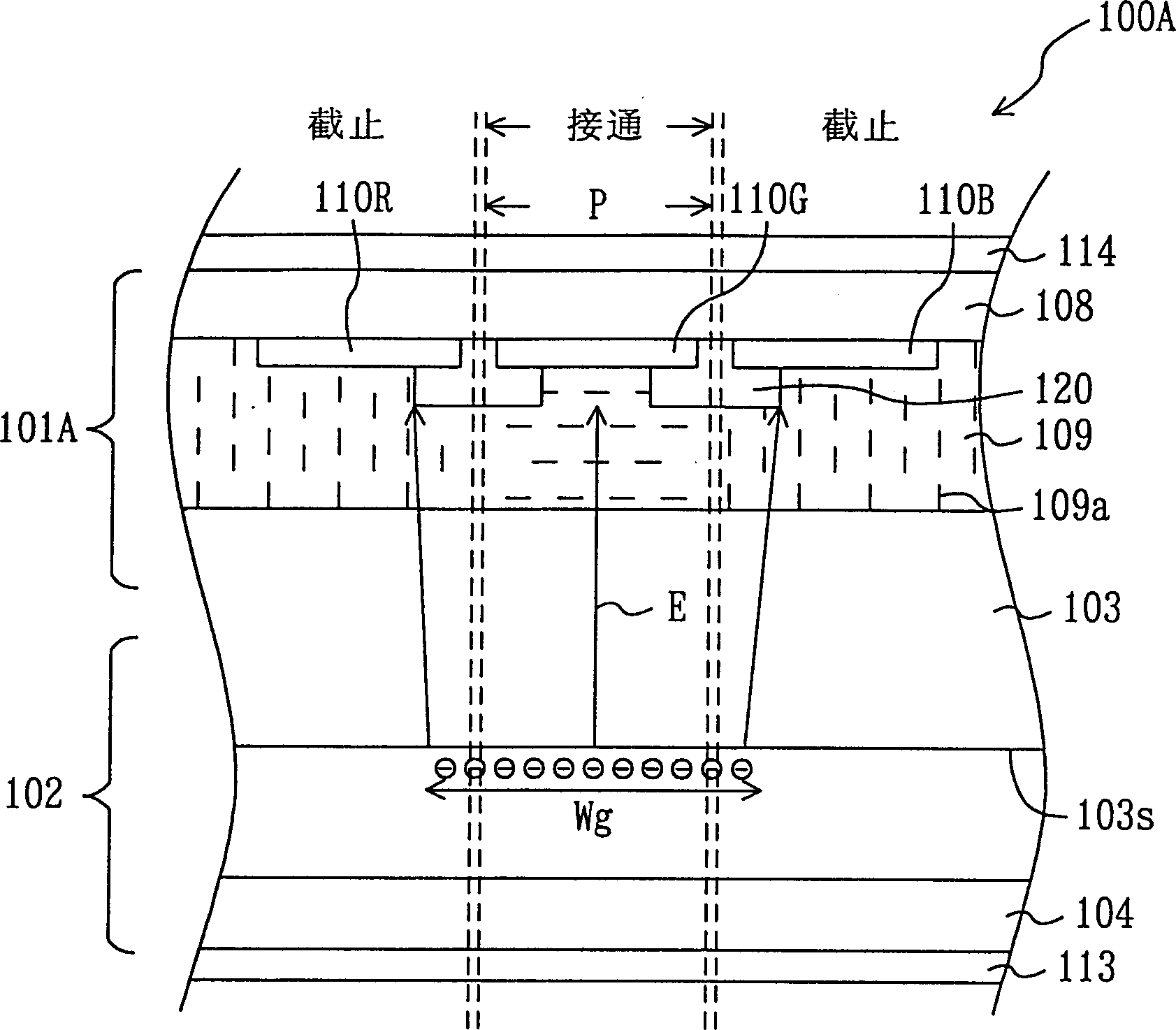
[0179] refer to Figure 8A , Figure 8B , Figure 8C and Figure 8D, the plasma addressing liquid crystal display 1100 in the second embodiment will be described. Like the conventional plasma-addressable liquid crystal display 1700 described above, the plasma-addressable liquid crystal display 1100 is also a liquid crystal display that uses vertically aligned negative dielectric anisotropic liquid crystal materials to display in a normally black mode. Figure 8A In the direction parallel to the extending direction of the plasma trench, the cross-sectional schematic diagram of the plasma addressing liquid crystal display 1100 in the embodiment of the present invention after cutting it, is equivalent to Figure 23A ; Figure 8B It is a cross-sectional schematic diagram of the plasma-addressed liquid crystal display 1100 after being cut in a direction perpendicular to the extending direction of the plasma trench; Figure 8C The above schematic diagram of the plasma addressin...
no. 3 Embodiment
[0219] With the configuration in the second embodiment, the phenomenon of crosstalk can be suppressed. However, if the width of the first dielectric structure formed at the edge region of the pixel region where the crosstalk phenomenon occurs becomes wider, the axis-symmetric arrangement of the liquid crystal molecules in the liquid crystal layer located on the first dielectric structure will be disordered, resulting in Display is uneven. Such a problem easily occurs when a flat region having a width of approximately 100 μm or more is formed on the first dielectric structure. This is because the alignment control force from other regions cannot sufficiently restrain the liquid crystal molecules on the flat region of the first dielectric structure so that the alignment is disordered.
[0220] Here, the plasma-addressed liquid crystal display in the third embodiment has a third dielectric structure formed on the first dielectric structure, and the third dielectric structure is ...
PUM
| Property | Measurement | Unit |
|---|---|---|
| thickness | aaaaa | aaaaa |
| thickness | aaaaa | aaaaa |
| thickness | aaaaa | aaaaa |
Abstract
Description
Claims
Application Information


