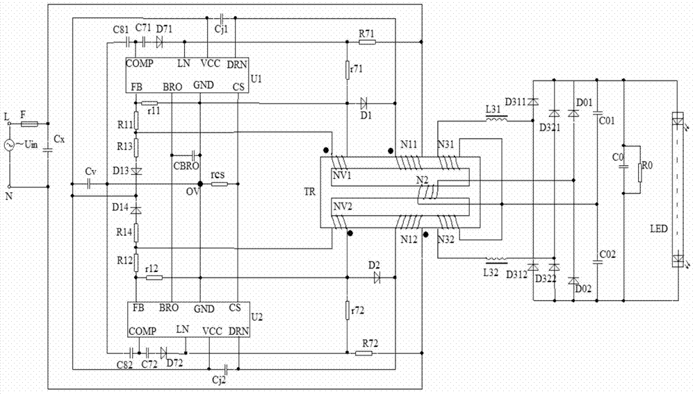
[0034] Combine below figure 1 The specific embodiments of the present invention will be further described.
[0035] Eliminate the constant current power supply for LED lamps with dimmable 12 volt incandescent lamps, including: AC power supply circuit, control circuit, coupling output circuit and ripple suppression circuit;
[0036] Such as figure 1 As shown, the magnetic integrated transformer TR used in the present invention includes a "日"-shaped magnetic core column, and the primary winding N11 and the primary winding N12 are respectively symmetrically wound around the two side columns of the "日"-shaped magnetic core column. Above, the secondary winding NV1 and the secondary winding NV2 are respectively symmetrically wound on the two side legs of the "日"-shaped magnetic core column, and the middle column secondary winding N2 is wound around the center column of the "日"-shaped magnetic core column. Above, the additional winding N31 and the additional winding N32 are respectively symmetrically wound on the two side legs of the "day"-shaped magnetic core leg.
[0037] The AC power supply circuit is connected to a 12 volt AC power source Uin, and includes a constant current drive chip U1 and a constant current drive chip controlled by the positive half wave and negative half wave polarity control of the 12 volt AC power source Uin to work alternately or rest half a wave respectively U2, and the alternating current positive half-wave current loop and the alternating current negative half-wave current loop controlled by the constant current drive chip U1 and the constant current drive chip U2 respectively.
[0038] The constant current driving chip U1 and the constant current driving chip U2 both use an integrated chip of the model DU8968 produced by Shanghai Duty Cycle Electronic Technology Co., Ltd.
[0039] The alternating current positive half-wave current loop is: in the positive half-wave of alternating current, the current flows from the positive terminal L of the 12 volt AC power supply Uin, and then flows through the fuse F, the synonymous terminal and the same terminal of the primary winding N11 in turn, and then It flows in from the DRN pin of the constant current drive chip U1, flows out from the CS pin, and then flows through the sampling resistor rcs, the common zero potential OV, the diode D2, the synonymous end and the same end of the primary winding N12 in turn, back to 12. The negative N terminal of the volt AC power supply Uin; controlled by the positive half-wave of the alternating current, the diode D1 is cut off, the diode D2 is turned on, the constant current driving chip U1 works, and the constant current driving chip U2 does not work;
[0040] The alternating current negative half-wave current loop is: in the negative half-wave of alternating current, the current flows from the negative N terminal of the 12 volt AC power supply Uin, flows through the same-named end and the different-named end of the primary winding N12 in turn, and then drives from a constant current The DRN pin of the chip U2 flows in and out from the CS pin, and then flows through the sampling resistor rcs, the common zero potential OV, the diode D1, the same-named and different-named ends of the primary winding N11, and the blown fuse F, back to 12. The positive polarity L terminal of the volt AC power supply Uin; controlled by the negative half-wave of the alternating current, the diode D2 is cut off, the diode D1 is turned on, the constant current driving chip U2 works, and the constant current driving chip U1 does not work.
[0041] The CS pin of the constant current drive chip U1 and the CS pin of the constant current drive chip U2 are simultaneously connected to one end of the sampling resistor rcs, and the other end of the sampling resistor rcs is connected to the common zero potential terminal OV. By selecting the sampling resistor rcs with different resistance values, it can be programmed to determine the output constant load current I led. rcs=0.2/I, where I is the expected constant current value, DU8968 specifies the upper limit peak value of I as 4A, and the threshold value (CS pin) voltage of the DU8968 built-in comparator is 0.2 volts.
[0042] The above-mentioned alternating current positive half-wave current loop and alternating current negative half-wave current loop are to adapt to the 12 volt low-voltage power supply Uin, eliminating the need for common AC power to be rectified by the bridge stack first, reducing the two PN junction voltage drops formed by the bridge stack rectification The loss is about 2 volts. For a 12 volt low-voltage power supply, the power loss is reduced by about 16%. The traditional AC-DC-AC-DC LED lamp power supply scheme is simplified to AC(AF)-AC(RF)-DC The LED lamp power supply scheme effectively improves the electrical efficiency and reduces the cost.
[0043] The control circuit includes a starting circuit for the constant current drive chip U1: in the positive half-wave of alternating current, the current flows from the positive L end of the 12 volt alternating current power source Uin, and then flows through the fuse F, the synonymous end of the primary winding N11 and The end with the same name, the starting capacitor Cj1, flows into the VCC pin of the constant current drive chip U1, and provides a current of more than 50 microamps to the VCC pin to start the constant current drive chip U1; after the constant current drive chip U1 starts, the secondary side The winding NV1 is connected in series with a 100R current limiting resistor R13 and a 4148 diode D13, and the secondary winding NV2 is connected in series with a 100R current limiting resistor R14 and a 4148 diode D14 to form a low-voltage power supply and self-powered to the constant current drive chip U1 The VCC pin supplies power and charges the energy storage capacitor Cv at the same time. The energy storage capacitor Cv can maintain a voltage of 12 volts for 20ms, which can maintain the constant current drive chip U1 to work normally.
[0044] The control circuit also includes a start-up circuit for the constant current drive chip U2: in the negative half-wave of alternating current, the current flows from the negative N terminal of the 12 volt alternating current power supply Uin, and then flows through the same-name end and the different-name end of the primary winding N12, The startup capacitor Cj2 flows into the VCC pin of the constant current drive chip U2, and provides a current of more than 50 microamps to the VCC pin to start the constant current drive chip U2; after the constant current drive chip U2 is started, the secondary winding NV1 string Connect the current limiting resistor R13 with model 100R and the 4148 diode D13, the secondary winding NV2 serially connect the current limiting resistor R14 with model 100R and the 4148 diode D14 to form a low-voltage power supply self-powered, and drive the VCC pin of the constant current drive chip U2 Power is supplied and the energy storage capacitor Cv is charged at the same time. The energy storage capacitor Cv can maintain a 12 volt voltage for 20ms, and the constant current drive chip U2 can be maintained to work normally.
[0045] The secondary winding NV1 and the secondary winding NV2 play the role of "primary feedback without optocoupler"; the induced voltage output by the secondary winding NV1 is fed back to the FB pin of the constant current drive chip U1 through the voltage division of the resistor R11 and the resistor r11, The induced voltage output by the secondary winding NV2 is fed back to the FB pin of the constant current drive chip U2 through the voltage divider of the resistor R12 and the resistor r12, and the constant current drive chip U1 and the constant current drive chip U2 are respectively controlled to work in the true "valley switch" Soft switch constant current state.
[0046] The LN pin of the DU8968 is the thyristor corner-cut sampling terminal. The input voltage of the 12V AC power supply Uin is fed back to the LN pin of the constant current drive chip U1 through the resistor R71 and the resistor r71. The input voltage is fed back to the LN pin of the constant current drive chip U2 through the resistor R72 and the resistor r72, and the dimming function is realized by the DU8968 internal microcircuit followed by the external circuit thyristor chopper voltage regulation. One end of the compensation capacitor CBRO is connected to the BRO pin of the constant current drive chip U1 and the BRO pin of the constant current drive chip U2, and the other end is connected to the common zero potential OV; when the external circuit thyristor dimming flickers, the compensation capacitor CBRO releases the charge make up.
[0047] A 103/15V compensation capacitor C81 is connected between the COMP pin and the GND pin of the constant current drive chip U1. At the same time, the COMP pin of the constant current drive chip U1 is connected to the anode of the diode D71 via the capacitor C71, and the cathode of the diode D71 is connected The LN pin of the constant current driver chip U1 is matched with the resistor R71 and the resistor r71 to divide the voltage, and the positive half-wave dimming and angle phase signal of the AC power is fed back to the LN pin of the constant current driver chip U1; the COMP of the constant current driver chip U2 The 103/15V compensation capacitor C82 is connected between the pin and the GND pin. At the same time, the COMP pin of the constant current drive chip U2 is connected to the anode of the diode D72 via the capacitor C72, and the cathode of the diode D72 is connected to the LN lead of the constant current drive chip U2. Pin; with resistor R72 and resistor r72 to divide the voltage, the negative half-wave dimming and cutting angle phase signal of the alternating current is fed back to the LN pin of the constant current drive chip U2. Play a role in suppressing flicker.
[0048] The coupling output circuit includes: one end of the middle column secondary winding N2 is simultaneously connected to one end of the energy storage capacitor C01 and one end of the energy storage capacitor C02, and the other end of the middle column secondary winding N2 is simultaneously connected to the anode of the rectifier diode D01 and the rectifier diode The cathode of D02, the other end of the energy storage capacitor C01 and the cathode of the rectifier diode D01 are all connected to the positive end of the load LED lamp, and the other end of the energy storage capacitor C02 and the anode of the rectifier diode D02 are all connected to the negative end of the load LED lamp; load LED The two ends of the lamp are also connected in parallel with an RC parallel filter circuit. The RC parallel filter circuit is composed of a parallel filter capacitor C0 and resistor R0. Flexible design of the number of turns of the secondary winding N2 of the middle column can be adapted to the LED lights of various voltage levels on the market.
[0049] The ripple suppression circuit includes: one end of the additional winding N31 is connected to the anode of the diode D311 and the cathode of the diode D312 after passing through the tuning inductor L31, and the other end is connected to one end of the additional winding N32 and connected to the energy storage capacitor C01 and the energy storage at the same time Between the capacitor C02, the other end of the additional winding N32 is connected to the anode of the diode D321 and the cathode of the diode D322 after passing through the tuning inductor L32. The cathode of the diode D311 and the cathode of the diode D321 are both connected to the anode of the load LED lamp and the anode of the diode 312 And the anode of the diode D322 are both connected to the cathode of the load LED lamp.
[0050] For a 50 Hz 12 volt AC power supply Uin, each half wave of AC occupies 10 milliseconds. Controlled by the positive and negative half-waves of the 12 volt AC power supply, the constant current drive chip U1 and the constant current drive chip U2 alternately work for half a wave (10 milliseconds), and alternately rest for half a wave (10 milliseconds). When the 12 volt alternating current crosses zero, the constant current driving chip U1 and the constant current driving chip U2 both stop working, forming an instantaneous dead zone period. At this time, the primary winding N11, starting capacitor Cj1, starting capacitor Cj2 and primary winding N12 are safe. The closed loop of capacitor Cx forms an LC series resonant circuit, which recovers power leakage inductance and distributed capacitance and stray electromagnetic field energy is induced to additional winding N31 and additional winding N32. Additional windings N31 and N32 are connected in series with inductor L31, inductor L32, capacitor C01 and capacitor C02 forms a "series resonant circuit", respectively tunes the two frequencies with greater harmonic energy in the power harmonic THD, so the originally harmful harmonic AC energy is converted into profit, and recycled into a DC current source. Supply power to the filter capacitor C0 and supply power to the load LED lights at the same time to smooth out the ripple of the output current. Therefore, it is not necessary to use a large-capacity electrolytic capacitor as a filter capacitor to achieve low LED ripple. If there are no additional windings N31 and N32, and only the middle column secondary winding N2 senses the energy output to the LED, then C0 needs a larger electrolytic capacitor, which can also achieve a 3% precision constant current for the LED, but the ripple Larger.