Frequency control system and method applied to power factor corrector
A technology of power factor correction and frequency control, applied in the frequency control field of frequency control system and power factor corrector, can solve the problems of reducing system power factor, etc. Effect
- Summary
- Abstract
- Description
- Claims
- Application Information
AI Technical Summary
Problems solved by technology
Method used
Image

Examples
Embodiment 1
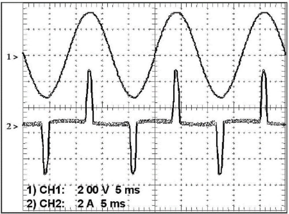
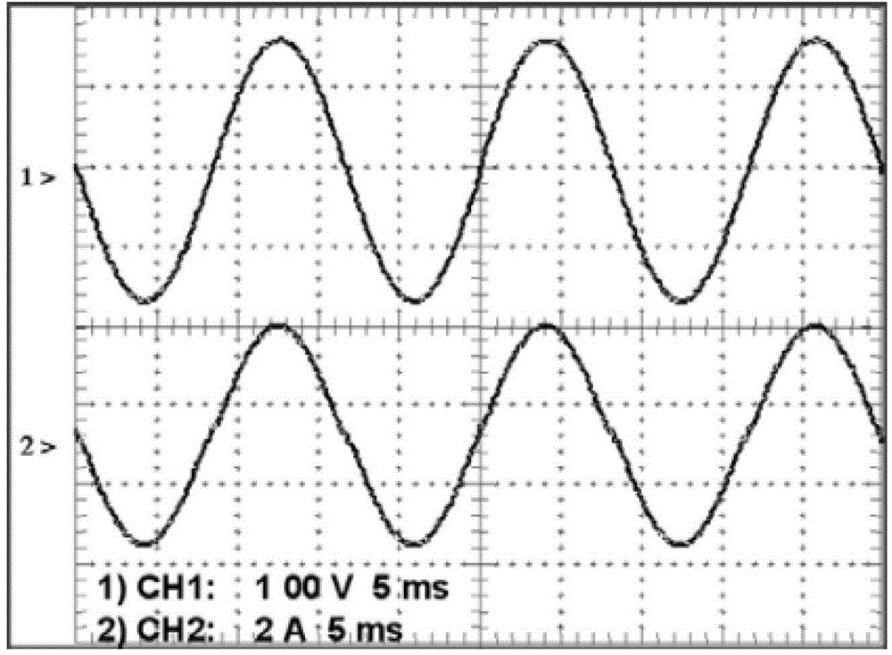
[0072] see Figure 10 , the present invention discloses a frequency control system applied to a power factor corrector, said system comprising: a zero current detector ZCD (zero current detector) 40, an analog multiplier 20, an error amplifier EA (Error amplifier) 10, a current Detection comparator 30, frequency corrector 50.
[0073] The output end of the error amplifier 10 is connected to an input end of the analog multiplier 20, the output end of the analog multiplier 20 is connected to an input end of the current detection comparator 30, and the output end of the current detection comparator 30 is connected to the frequency corrector 50. One input terminal, the output terminal of the zero current detector 40 is connected to one input terminal of the frequency corrector 50 .
[0074] The zero current detector 40 is used to detect the boost inductor of the power factor corrector PFC ( Figure 6 In L1), when the boost inductor current drops to zero, a new switching cycle ...
Embodiment 2
[0088] see Figure 13 The difference between this embodiment and Embodiment 1 is that in this embodiment, the frequency corrector includes an RS flip-flop 53 , an adjustable timer 51 , and a logical OR gate 52 . The adjustable timer 51 receives the MULT voltage and a reset signal, and the reset signal comes from the output PFC power tube control signal. The output signal of the adjustable timer 51 is connected to one input terminal of the logical OR gate 52 , and the output signal of the zero current detector 40 is connected to the other input terminal of the logical OR gate 52 . The output signal of the logical OR gate 52 is connected to an input terminal of the RS flip-flop 53 , and the output signal of the current detection comparator 30 is connected to an input terminal of the RS flip-flop 53 .
[0089] see Figure 14 , the adjustable timer 51 includes a constant current source I1, a first capacitor C1, a reset switch S1 and its control input signal, a comparator with hy...
PUM
 Abstract
Description
Claims
Application Information