Interconnection structure and forming method of interconnection structure

A technology of interconnection structure and single-layer structure, applied in electrical components, electric solid devices, circuits, etc., can solve problems such as poor interconnection structure performance and device failure, achieve performance improvement, reduce copper accumulation phenomenon, and improve electromigration. Effects of Features

Active Publication Date: 2015-01-21
SEMICON MFG INT (SHANGHAI) CORP
View PDF7 Cites 2 Cited by
  • Summary
  • Abstract
  • Description
  • Claims
  • Application Information

AI Technical Summary

Problems solved by technology

[0005] Although SiCN, as the cap layer of the interconnection structure, can reduce copper diffusion to a certain extent, the interconnection structure formed by the prior art still has the problem o...

Method used


Image

  • Interconnection structure and forming method of interconnection structure
  • Interconnection structure and forming method of interconnection structure
  • Interconnection structure and forming method of interconnection structure

Examples


Embodiment Construction

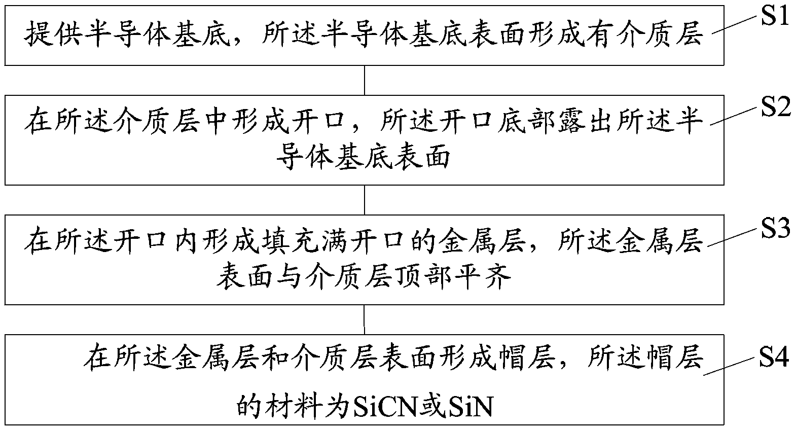
[0037] It can be seen from the background art that the copper accumulation problem of the interconnection structure formed in the prior art has the problem of copper accumulation, and the performance of the formed interconnection structure is low.

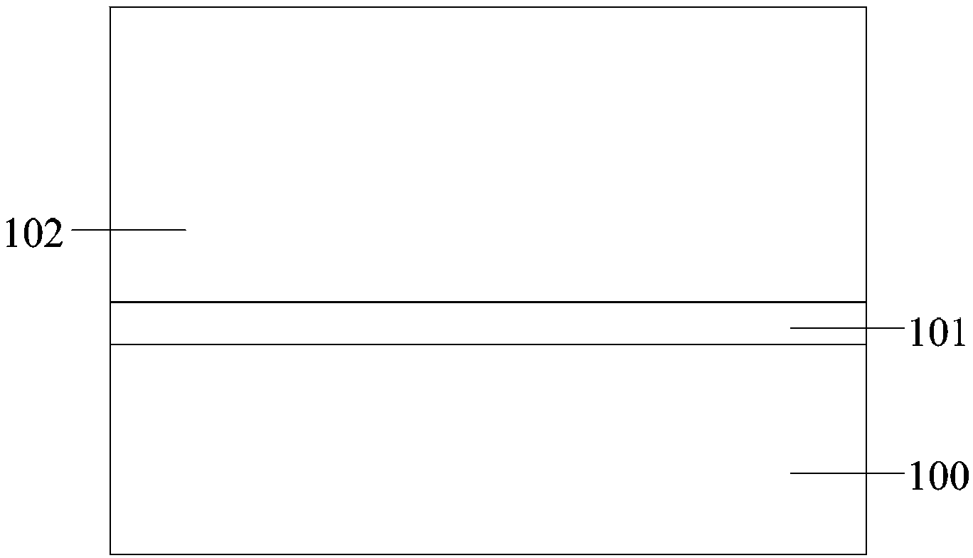
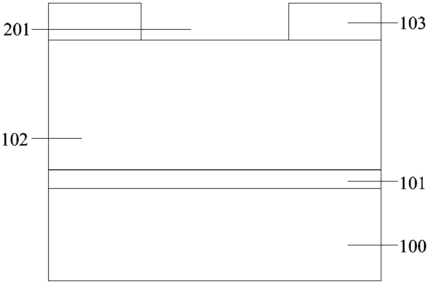
[0038] In order to solve the above problems, research on the formation process of the interconnection structure, please refer to figure 1 : step S1, providing a semiconductor substrate, a dielectric layer is formed on the surface of the semiconductor substrate; step S2, forming an opening in the dielectric layer, and the bottom of the opening exposes the surface of the semiconductor substrate; step S3, forming a The metal layer that fills the opening, the surface of the metal layer is flush with the top of the dielectric layer; step S4, forming a cap layer on the surface of the metal layer and the dielectric layer, and the material of the cap layer is SiCN or SiN.

[0039] The relative permittivity of SiCN or SiN is small (SiCN has...


PUM

PropertyMeasurementUnit
Thicknessaaaaaaaaaa
Thicknessaaaaaaaaaa

Abstract

The invention discloses an interconnection structure and a forming method of the interconnection structure. The forming method of the interconnection structure comprises the following steps: providing a semiconductor substrate, wherein a dielectric layer is formed on the surface of the semiconductor substrate; forming an opening in the dielectric layer, wherein the bottom of the opening is exposed out of the surface of the semiconductor substrate; forming a metal layer filling the opening in the opening, wherein the surface of the metal layer is flush with the top of the dielectric layer; forming a first cap layer on the surfaces of the metal cap layer and the dielectric layer, wherein the first cap layer is made from SiBC; and forming a second cap layer on the surface of the first cap layer. Through adoption of the forming method, the occurrence probability of a copper accumulation phenomenon in the interconnection structure is lowered; the electromigration service life of the interconnection structure is prolonged; and the reliability of the interconnection structure is enhanced.

Description

technical field [0001] The invention relates to the field of semiconductor manufacturing, in particular to an interconnection structure and a method for forming the interconnection structure. Background technique [0002] With the continuous advancement of VLSI process technology, the feature size of semiconductor devices has been continuously reduced, and the performance of semiconductor devices has become stronger and stronger. However, as the size of semiconductors continues to shrink, smaller and smaller interconnect structures carry higher and higher currents, and the response time requirements of interconnect structures are getting shorter and shorter. Traditional aluminum interconnect structures can no longer meet the requirements. Compared with aluminum, metal copper has lower resistivity and better resistance to electromigration. The copper interconnect structure can reduce the resistance-capacitance (RC) delay of the interconnect structure, improve electromigration...

Claims


Application Information

Patent Timeline
IPC IPC(8): H01L23/538H01L21/768
Inventor 邓浩
Owner SEMICON MFG INT (SHANGHAI) CORP
Why Eureka
Try Eureka