Forming method of copper-interlinked dielectric covering layer

A dielectric and covering layer technology, which is applied in the field of forming a dielectric covering layer, can solve problems such as the influence of copper interconnection electromagnetic characteristics, achieve the effects of improving electromigration characteristics, improving reliability and yield, and improving interface characteristics

Active Publication Date: 2017-01-25
SEMICON MFG INT (SHANGHAI) CORP
View PDF4 Cites 0 Cited by
  • Summary
  • Abstract
  • Description
  • Claims
  • Application Information

AI Technical Summary

Problems solved by technology

Unsmooth interfaces will have a greater impact on the electromagnetic properties of copper interconnects

Method used


Image

  • Forming method of copper-interlinked dielectric covering layer
  • Forming method of copper-interlinked dielectric covering layer
  • Forming method of copper-interlinked dielectric covering layer

Examples


Embodiment Construction

[0030] In the following description, a lot of specific details are given in order to provide a more thorough understanding of the present invention. However, it is obvious to those skilled in the art that the present invention can be implemented without one or more of these details. In other examples, in order to avoid confusion with the present invention, some technical features known in the art are not described.

[0031] In order to thoroughly understand the present invention, detailed steps and detailed structures will be proposed in the following description to explain the technical solution proposed by the present invention. The preferred embodiments of the present invention are described in detail as follows. However, in addition to these detailed descriptions, the present invention may also have other embodiments.

[0032] It should be understood that the present invention can be implemented in different forms and should not be construed as being limited to the embodiments...


PUM

PropertyMeasurementUnit
thicknessaaaaaaaaaa

Abstract

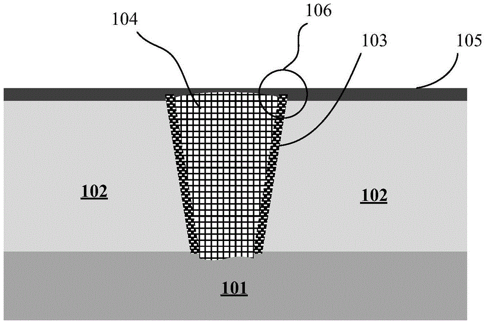
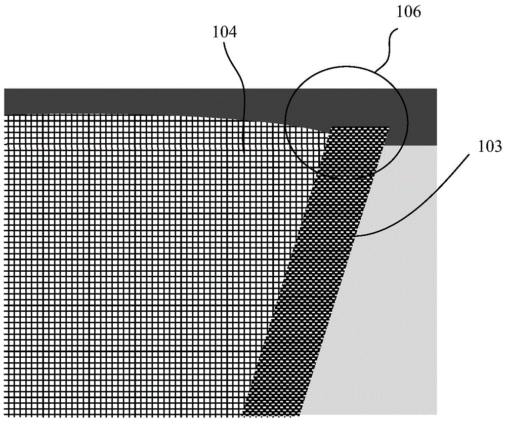
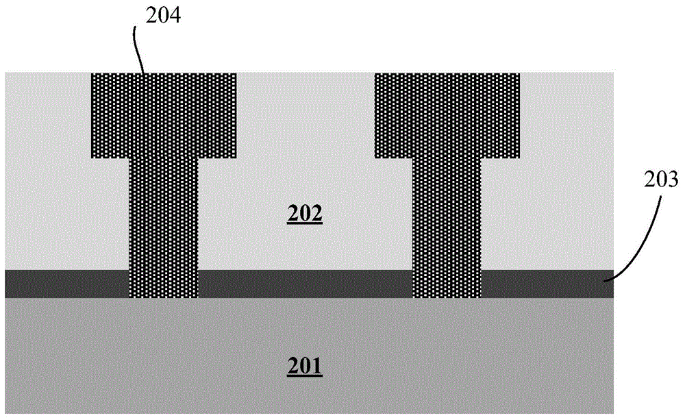
The invention provides a forming method of a copper-interlinked dielectric covering layer. The forming method includes: providing a semiconductor substrate; forming a low K dielectric layer and a copper-interlinked structure positioned in the low K dielectric layer on the semiconductor substrate; etching the low K dielectric layer to enable height of the top face of the low K dielectric layer to be smaller than that of the top face of the copper-interlinked structure; depositing an amorphous Si layer on the surface of the low K dielectric layer and the copper-interlinked structre; introducing a first gas source to treat the amorphous Si layer to form a silicon-enriched SiN layer; performing annealing treatment to form a CusiN layer on the surface of the copper-interlinked structure; introducing a second gas source to treat the surfaces of the low K dielectric layer and the copper-interlinked structure to enable the amorphous Si layer to be completely converted into a SiN layer and to fully form the CuSiN layer on the surface of the copper-interlinked structure; depositing on the SiN layer to form the dielectric covering layer. By the forming method, reliability of devices can be ensured, electromigration characteristics of copper interlinking are improved, influence on electromagnetic characteristics of copper interlinking is avoided, and the problem that bad influence is generated on the electromagnetic characteristics due to the fact that an interface covered by a sharp corner is uneven is solved.

Description

Technical field [0001] The present invention relates to a semiconductor manufacturing process, in particular to a method for forming a copper interconnect dielectric covering layer. Background technique [0002] With the development of integrated circuits, the feature size continues to decrease, and the current density of metal wires increases sharply. At the same time, the increase in chip integration leads to an increase in power consumption per unit area. Therefore, the reliability of metal connections has always been an IC design And manufacturing concerns. In the metal wire, the electrons moving in the opposite direction of the electric field exchange momentum with the metal ions, resulting in the mass transport of the metal ions dominated by diffusion. This phenomenon is called electromigration. Electromigration is an important metal failure mechanism in the interconnect structure of semiconductor devices. There are two types of failures caused by electromigration, namely...

Claims


Application Information

Patent Timeline
Patent Type & Authority Applications(China)
IPC IPC(8): H01L21/768
CPCH01L21/76829
Inventor 邓浩
Owner SEMICON MFG INT (SHANGHAI) CORP
Why Eureka
Try Eureka