Method for manufacturing photovoltaic module

a photovoltaic module and manufacturing method technology, applied in the field of photovoltaic module manufacturing, can solve the problems of deteriorating output characteristics, more cracks or warpage in cells, and deteriorating output characteristics, so as to improve the interface properties of solar cells, improve the output thereof, and improve the effect of solar cell characteristics

Inactive Publication Date: 2010-07-13
SANYO ELECTRIC CO LTD
View PDF7 Cites 15 Cited by
  • Summary
  • Abstract
  • Description
  • Claims
  • Application Information

AI Technical Summary

Benefits of technology

[0018]In view of the above problems, inventors of the present invention considered and investigated thoroughly the solar cell after the collector electrode is formed, and found that optimally controlled heating temperature and heating time would improve the output characteristics.
[0034]It is assumed that the above discussed configuration of this invention can improve the interface properties of the solar cell, therefore improving the output thereof, and also make an interconnection under accurate temperature control. Consequently, the present invention can provide a method for manufacturing the photovoltaic module with good solar cell characteristics and high yield.

Problems solved by technology

This scheme has an advantage of a relatively quick temperature rise; however, exact heat control is difficult, therefore causing more cracks or warpage in the cells.
However, the solar cell having the amorphous silicon layer formed through the CVD method have the output characteristics deteriorate if heated for a long time at a temperature as high as 200 degrees Celsius or more.
However, the solar cell having the amorphous silicon layer formed through the CVD method may have the output characteristics deteriorate due to being heated for a long time at high temperatures.
For this reason, there is no adequate consideration for the heat treatment for improving the output characteristics of the solar cells.

Method used


Image

  • Method for manufacturing photovoltaic module
  • Method for manufacturing photovoltaic module
  • Method for manufacturing photovoltaic module

Examples


Embodiment Construction

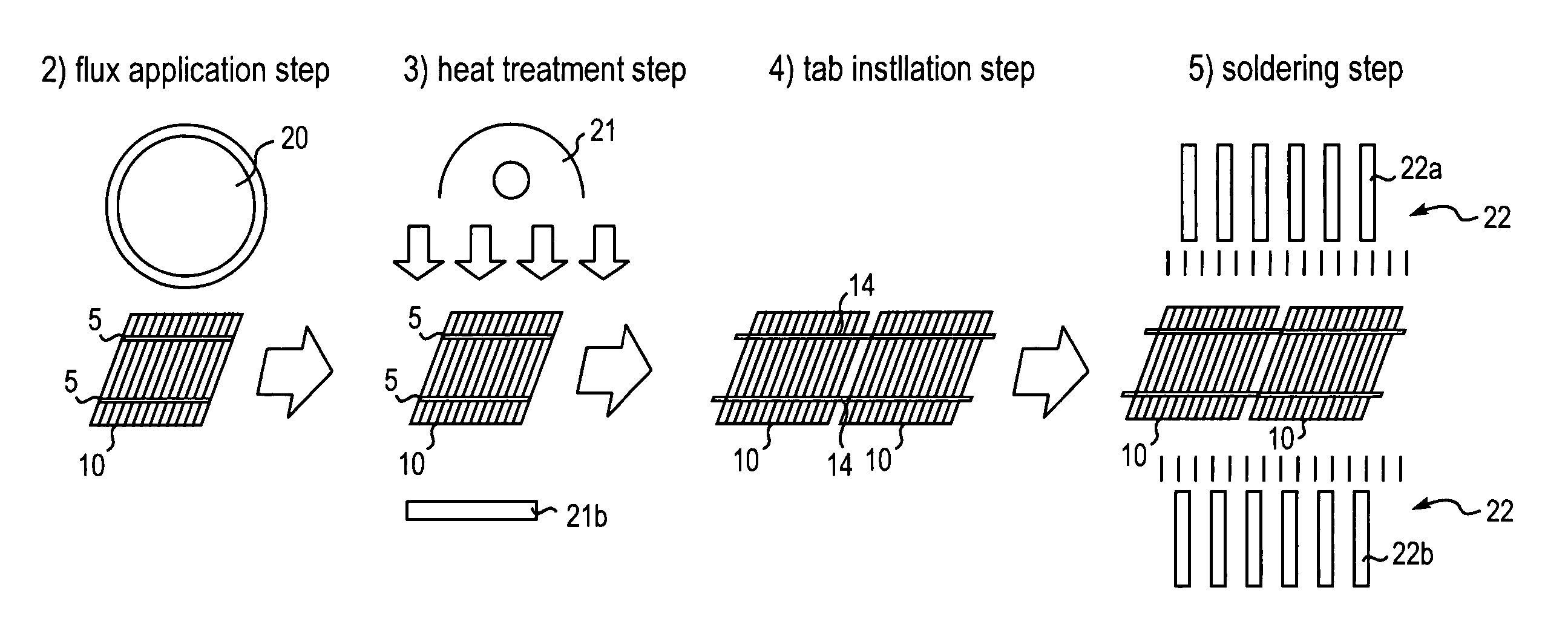
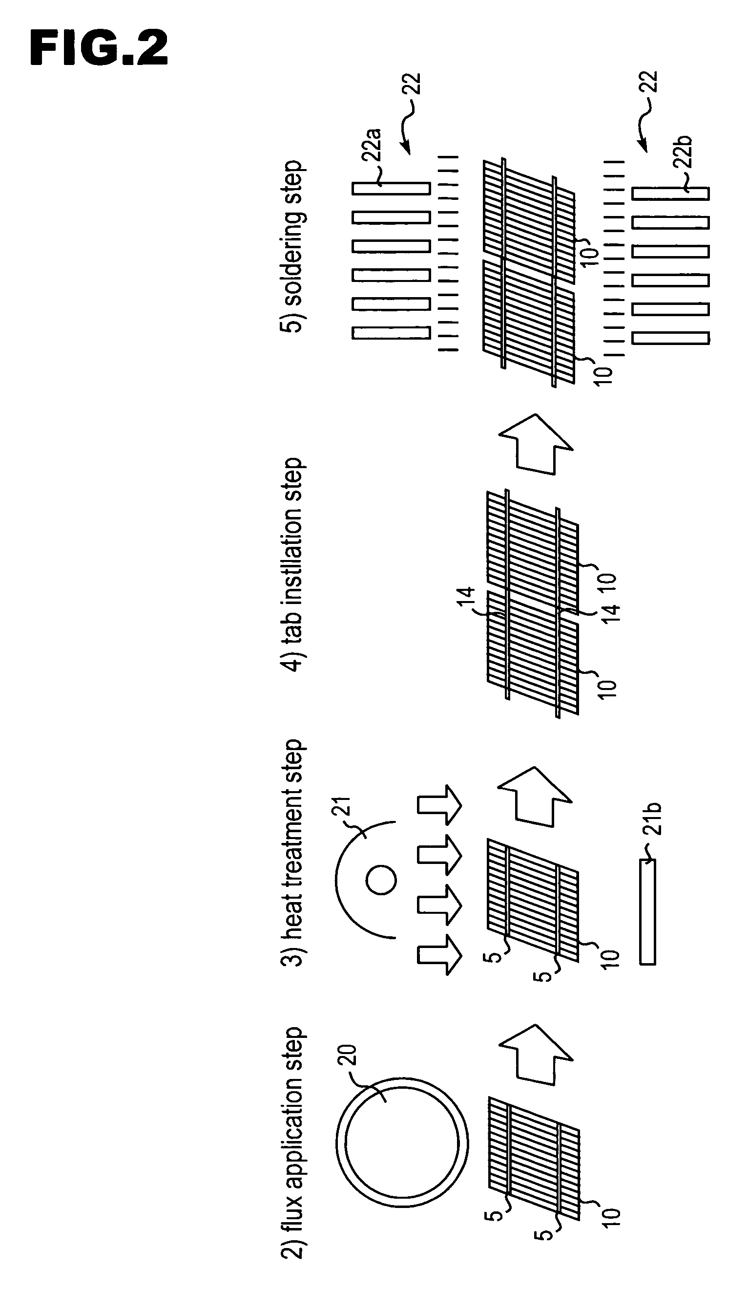
[0049]With reference to the drawings, detailed descriptions will be made on an embodiment of the present invention. Components identical or equivalent to each other in the drawings are denoted the same reference number, and will not be further explained to avoid repetition.

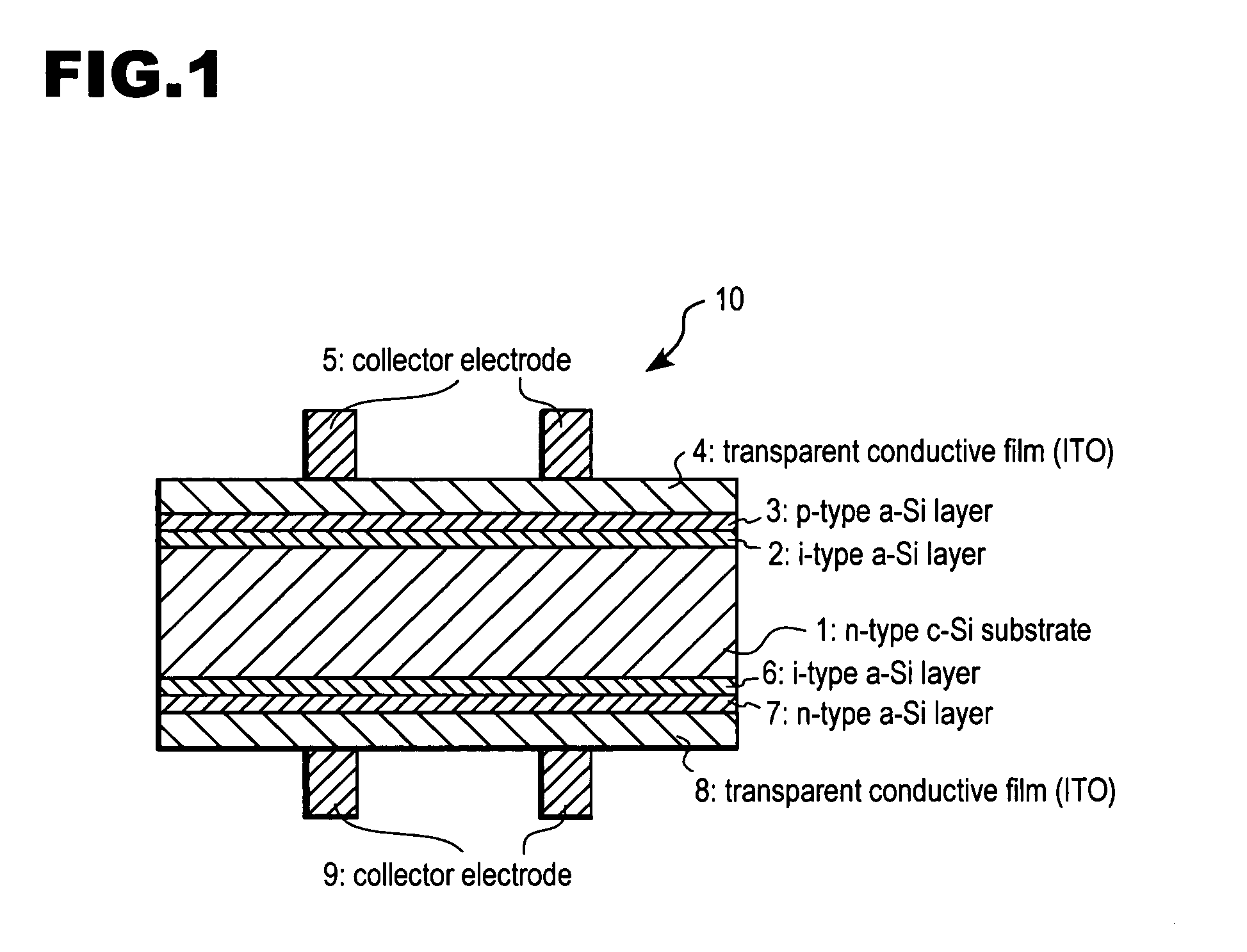
[0050]Firstly, an example of the solar cell to which this invention is applied will be described by referring to FIG. 1. The solar cell 10, as shown in FIG. 1, includes an n-type single-crystal silicon substrate 1 having a thickness of 100 μm to 300 μm and (100) planes (hereinafter referred to as “n-type single-crystal silicon substrate 1) as a crystalline semiconductor substrate. On the surface of the n-type single-crystal silicon substrate 1, there formed pyramidal projections and depressions having a height of a few micro meters to a few tens of micro meters for confining light. A substantially intrinsic i-type amorphous silicon (a-Si:H) layer 2 having a thickness of a few nanometers to a few tens of nanometers...


PUM


Abstract

This invention is made to improve the characteristics of a photovoltaic module in which a plurality of solar cells are electrically connected to each other with connecting members such as tabs or connecting leads. The present invention provides a method for manufacturing a photovoltaic module comprising a plurality solar cells each including a semiconductor heterojunction made by combining amorphous silicon and crystalline silicon and connecting members for connecting the plurality solar cells in which the connecting members are connected to the solar cells by soldering after a high-temperature heat treatment is applied to the solar cells, and the plurality of solar cells are electrically connected to each other with the connecting members.

Description

[0001]This application claims priority in foreign applications Number JP2005-176718 and JP2006-098248.BACKGROUND OF THE INVENTION[0002]1. Field of the Invention[0003]This invention relates to a method for manufacturing photovoltaic modules, in particular, relates to a method for manufacturing a photovoltaic module in which a plurality of solar cells are electrically connected to each other by connecting members referred to as connecting tabs, connecting leads, or the like.[0004]2. Description of Related Art[0005]With the recent growing expectation on clean energy to solve the global environment conservation issues such as the global warming, attention is being given to solar batteries, as a clean energy source, which directly convert sunlight into electric energy. Typical photovoltaic devices using these solar batteries for power generation include a plurality of solar cells and are configured to electrically connect the adjacent solar cells to each other in series or in parallel by...

Claims


Application Information

Patent Timeline
Patent Type & Authority Patents(United States)
IPC IPC(8): H01L31/042
CPCH01L31/0747H01L31/188H01L31/0504Y02E10/50H01L31/208Y02P70/50
Inventor OKAMOTO, SHINGOYAGIURA, TOSHIO
Owner SANYO ELECTRIC CO LTD
Why Eureka
Try Eureka