Heating device for semiconductor packaging wire bonding process and fixture thereof

A heating device and semiconductor technology, applied in the fields of semiconductor devices, semiconductor/solid-state device manufacturing, and electric solid-state devices, etc., can solve the problems of surface contamination of pads, degradation of bonding properties of wires 34, and influence on the surface of wire bonding positions.

Inactive Publication Date: 2011-07-27
ASE ASSEMBLY & TEST SHANGHAI
View PDF0 Cites 7 Cited by
  • Summary
  • Abstract
  • Description
  • Claims
  • Application Information

AI Technical Summary

Problems solved by technology

[0006] However, the design of the heating device 1 of the lead frame bar 2 has the following disadvantages: when the heating block 11 heats the lead frame bar 2, since the upper surface of the heating block 11 is a flat surface, Therefore, the contact area between the heating block 11 and the lead frame bar 2 includes the entire upper surface of the heating block 11, and a part of the heat energy of the heating block 11 will be absorbed by the lead frame bar 2 without wiring. Peripheral area (such as the inner pin portion 22 and chip seat 21 of the next lead frame unit on the left that has not yet been wired, or the inner pin portion 22 and chip seat of the previous lead frame unit that has completed wiring on the right 21) absorbed, thus causing the inner pin portion 22 in the wire bonding window 12a of the fixture 12 to take a longer heating time to reach the required wire bonding temperature
However, the flat design of the upper surface of the heating block 11 of the heating device 1 for the packaging substrate is also easy to overheat the surrounding area (such as the next packaging substrate unit on the left that has not yet been wired, or the front that has completed the wiring on the right). A packaging substrate unit) metal oxidation on the pad surface of the finger area 32 (and the pad surface of the semiconductor chip 33), which in turn affects the bonding properties of the wire bonding position surface and the wire 34, and the subsequent encapsulation. Yield rate, and also the problem of organic volatile gas causing surface contamination of pads

Method used


Image

  • Heating device for semiconductor packaging wire bonding process and fixture thereof
  • Heating device for semiconductor packaging wire bonding process and fixture thereof
  • Heating device for semiconductor packaging wire bonding process and fixture thereof

Examples


Embodiment Construction

[0030] In order to make the above-mentioned purposes, features and advantages of the present invention more obvious and understandable, the preferred embodiments of the present invention will be specifically cited below, together with the accompanying drawings, for a detailed description as follows:

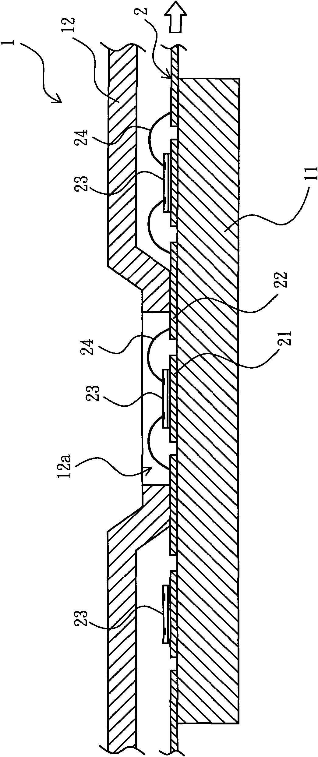
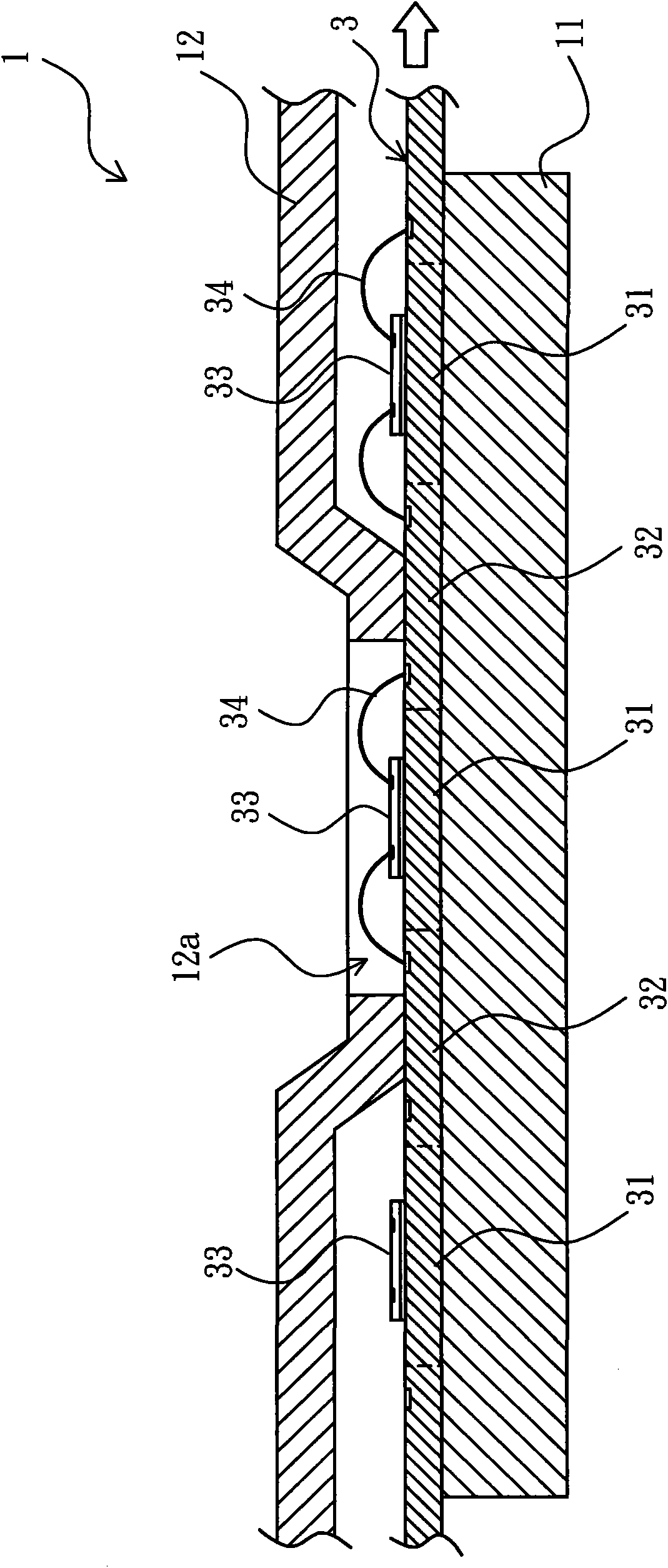
[0031] The heating device and method of the package wire bonding process provided by the present invention are mainly used for temporarily carrying and clamping and heating a package carrier such as a leadframe (leadframe) or packaging substrate (substrate) during the wire bonding process, so as to improve the wire bonding process. The quality of the joint.

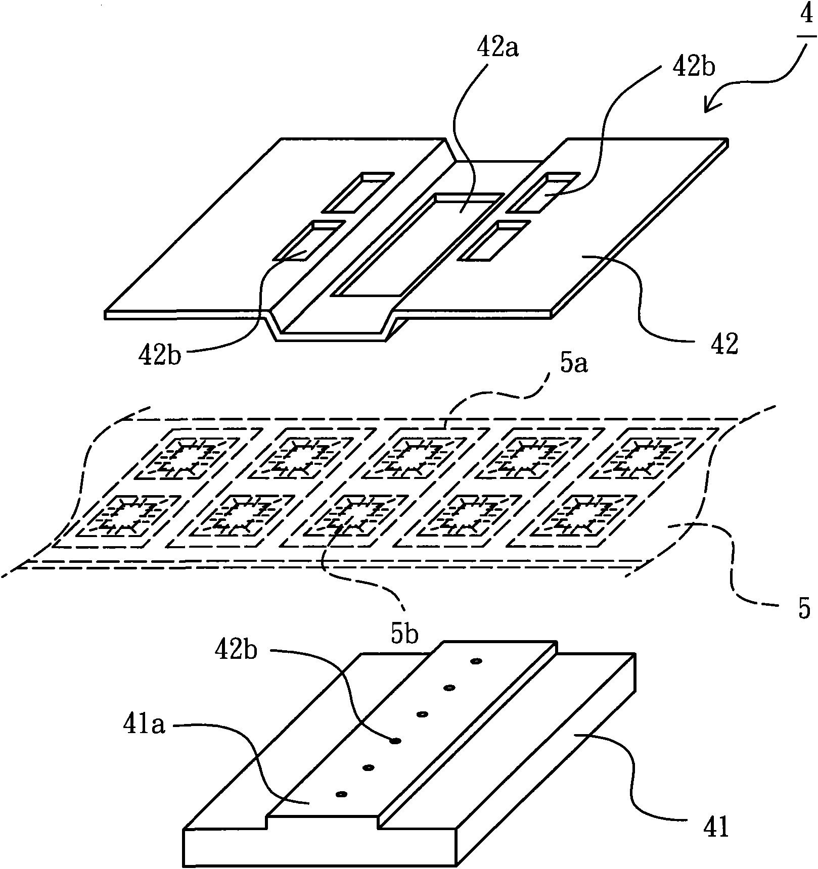
[0032] Please refer to image 3 As shown, the heating device 4 of the semiconductor package wire bonding process according to the first embodiment of the present invention mainly includes: a heating block 41 and a clamp 42 . The clamp 42 is located above the heating block 41 , and the clamp 42 is used for clamping and posit...


PUM


Abstract

The invention discloses a heating device for a semiconductor packaging wire bonding process and a fixture thereof. The heating device comprises a heating block and a fixture. The heating block comprises a convex part which is convexly arranged on the upper surface of the heating block and used for bearing a wire bonding operation area of a packaging carrier; the fixture is positioned above the heating block and used for clamping the packaging carrier; and the packaging carrier is clamped and positioned between the heating block and the fixture. The fixture comprises a wire bonding window and at least an exhaust port. The wire bonding window exposes the wire bonding operation area on the packaging carrier; and the exhaust port is arranged at least one side of the wire bonding window. Therefore, the heating device can perform centralized heating on the wire bonding operation area by use of the convex part so as to reduce the heating time and prevent metal oxidation of the surface on the wire bonding position caused by excessive heating, and can exhaust organic volatile gas generated by wire bonding through the exhaust port so as to avoid pollution on the surface of the wire bonding position.

Description

【Technical field】 [0001] The present invention relates to a heating device and a fixture for a semiconductor packaging wire bonding process, in particular to a heating device and a fixture for a semiconductor packaging wire bonding process that can prevent the surface oxidation of the wire bonding position caused by overheating and avoid contamination by organic volatile gases. its fixture. 【Background technique】 [0002] The semiconductor packaging process is used to provide a packaging structure to protect a semiconductor chip, so that the semiconductor chip can avoid external force impact, dust pollution, moisture or oxidation when it is powered on, so that the packaging structure can be used to improve the reliability of the semiconductor chip and prolong the life of the semiconductor chip. its service life. In the existing manufacturing process of semiconductor packaging, semiconductor wafers are usually obtained first and wafer tests are performed on them. After passi...

Claims


Application Information

Patent Timeline
Patent Type & Authority Applications(China)
IPC IPC(8): H01L21/683H01L21/60
CPCH01L2224/85H01L2924/01082H01L2924/01047H01L2924/01079H01L2224/97H01L2224/48465H01L2224/32245H01L2224/48247H01L2224/48227H01L24/85H01L2924/01322H01L2924/01033H01L2924/01006H01L2924/01029H01L24/78H01L2224/78703H01L2224/48091H01L2224/73265H01L2924/01013H01L2224/45147H01L2224/85181H01L2224/32225H01L2224/92247H01L2224/78301H01L2924/181H01L24/73H01L2924/10161H01L2224/78H01L2224/45H01L2924/00014H01L2224/83H01L2924/00H01L2924/00012
Inventor 刘怡
Owner ASE ASSEMBLY & TEST SHANGHAI
Why Eureka
Try Eureka