Method for forming cell capacitor for high-integrated DRAMs

a cell capacitor and high-integration technology, applied in the direction of capacitors, semiconductor devices, electrical apparatus, etc., can solve the problems of high leakage current in the subsequent process, difficulty in high-integration of capacitors, and limit on storing charge, so as to improve the interfacial properties of aluminum oxide, prevent leakage current excellent, and high capacitance

a cell capacitor and high-integration technology, applied in the direction of capacitors, semiconductor devices, electrical apparatus, etc., can solve the problems of high leakage current in the subsequent process, difficulty in high-integration of capacitors, and limit on storing charge, so as to improve the interfacial properties of aluminum oxide, prevent leakage current excellent, and high capacitance

US20020094624A1Inactive Publication Date: 2002-07-18SK HYNIX INC

Image

  • Method for forming cell capacitor for high-integrated DRAMs
  • Method for forming cell capacitor for high-integrated DRAMs
  • Method for forming cell capacitor for high-integrated DRAMs

Examples


Embodiment Construction

[0015] Preferred embodiments will now be described with reference to the accompanying drawings.

[0016] FIGS. 1a through 1d are cross-sectional views sequentially illustrating a method for forming a cell capacitor used for a high-integrated DRAM in accordance with the disclosed methods.

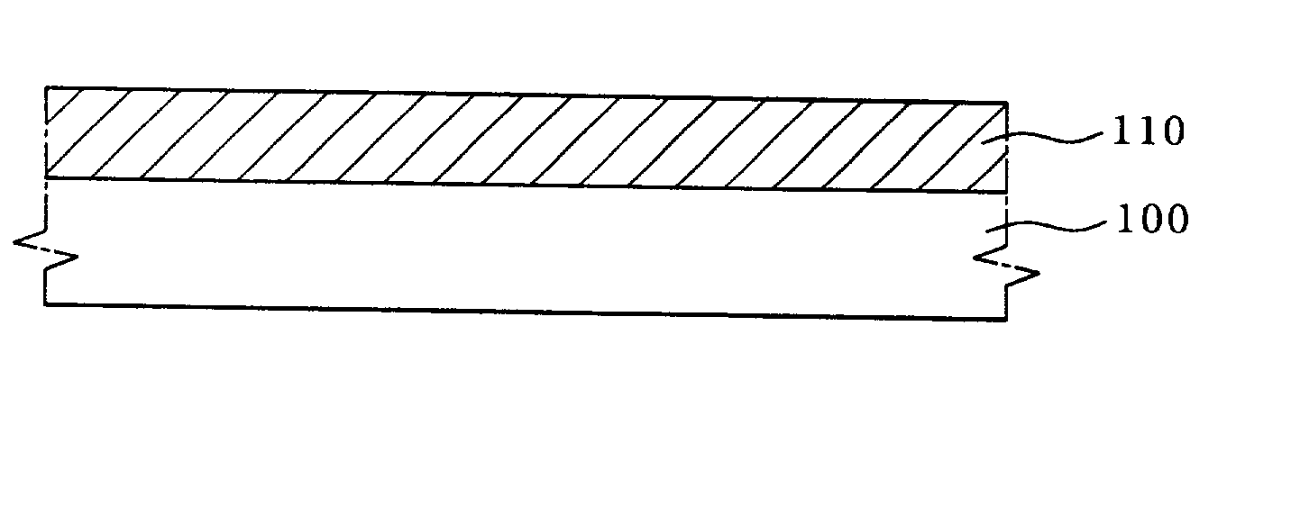
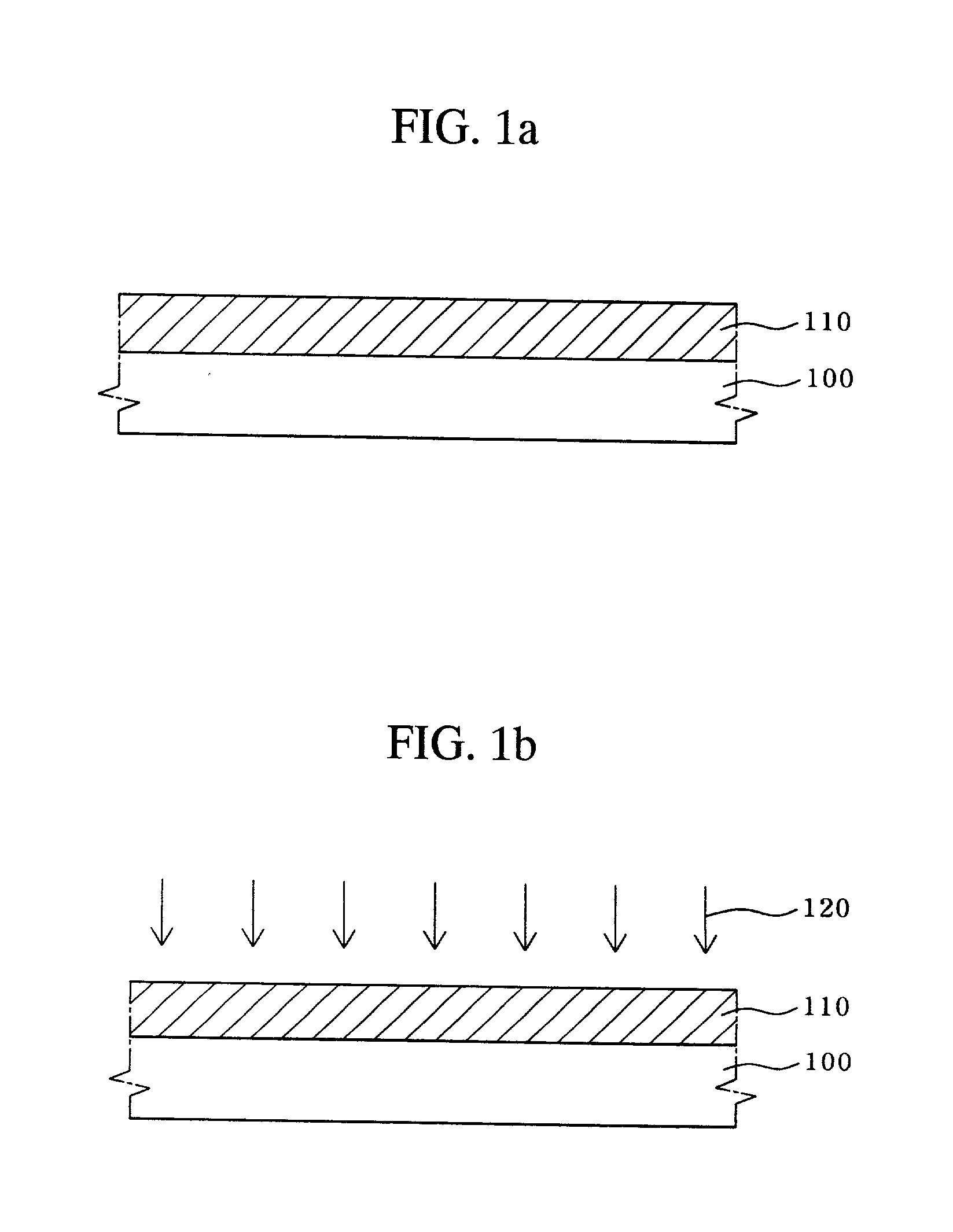
[0017] As illustrated in FIG. 1a, aluminum oxide is deposited as a first dielectric layer 110 on a semiconductor substrate 100 having a predetermined lower substructure by an ALD (atomic layer deposition) method.

[0018] At this time, the first dielectric layer 110 is deposited on the semiconductor substrate 100 heated at a temperature ranging from about 200 to about 450.degree. C. in a chamber having a pressure ranging from about 0.1 to about 1 Torr by using vapor.

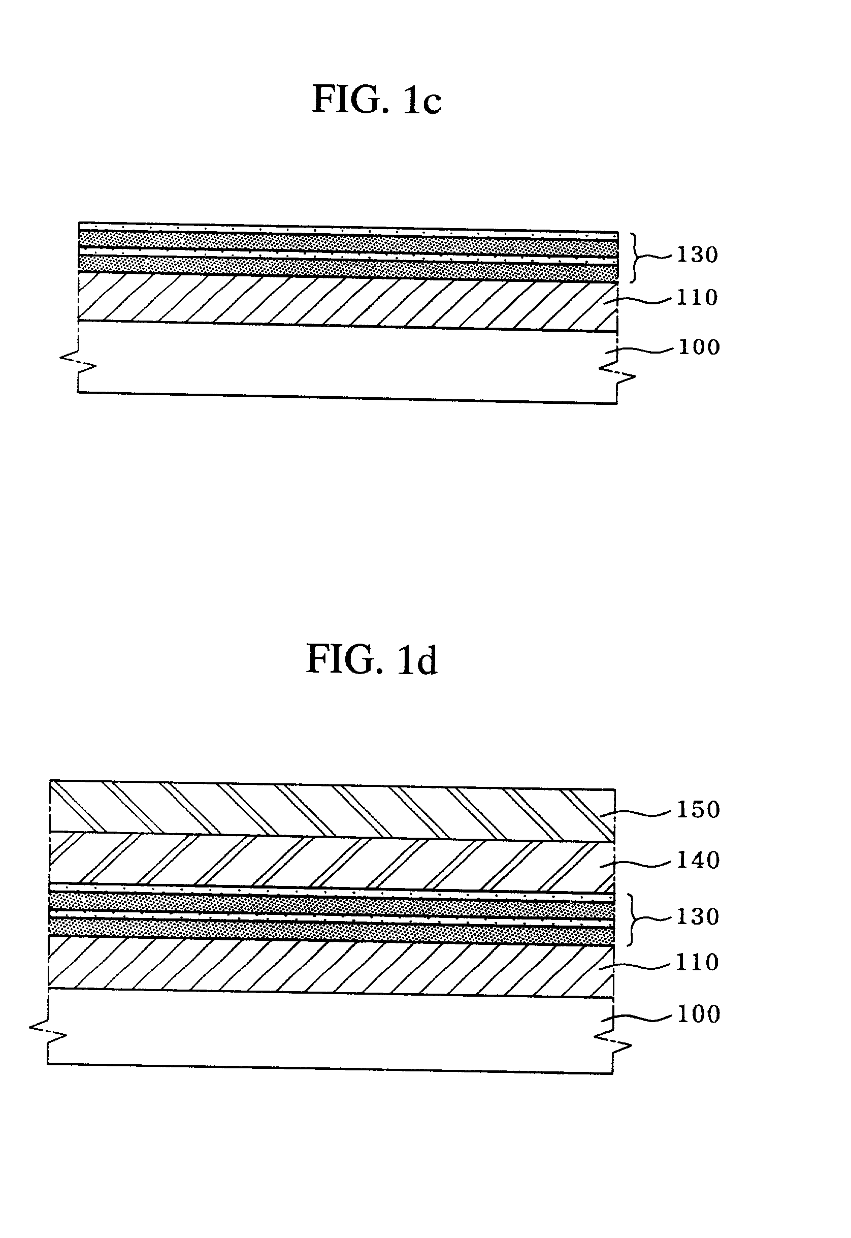
[0019] Then, as illustrated in FIG. 1b, carbon and impurities in the aluminum oxide are removed by performing a N.sub.2O plasma annealing process 120 on the resultant material at a temperature ranging from about 300 to about 400.degree. C., and...


PUM

PropertyMeasurementUnit
pressureaaaaaaaaaa
temperatureaaaaaaaaaa

Abstract

A method for forming a cell capacitor used for a high-integrated DRAM is disclosed which guarantees interfacial properties of aluminum oxide and excellent leakage current preventive properties by depositing an aluminum oxide layer and a mixed layer of TiON and TiO2 as dielectric layers on a semiconductor substrate having a predetermined lower substructure by an atomic layer deposition (ALD) method and thus forming a double layer structure, and simultaneously providing a high capacitance by using a high dielectric property of a mixed layer of TiON and TiO2.

Description

[0001] 1. Technical Field[0002] A method for forming a cell capacitor for a high-integrated DRAM which provides good interfacial properties of aluminum oxide and excellent leakage current preventive properties by depositing an aluminum oxide layer and a mixed layer of TiON and TiO.sub.2 as dielectric layers on a semiconductor substrate having a predetermined lower substructure by an atomic layer deposition (ALD) method and thus forming a double layer structure, and simultaneously providing a high capacitance by using a high dielectric property of a mixed layer of TiON and TiO.sub.2.[0003] 2. Description of the Related Art[0004] Recently, with the development of semiconductor integrated circuit processing techniques, the minimum line width of a device manufactured on a semiconductor substrate is getting miniaturized and unit area integration degree is getting increased. Meanwhile, as the integration degree of a memory cell increases, a space occupied by a cell capacitor for charge st...

Claims


Application Information

Patent Timeline
18 Jul 2002
Publication
US20020094624A1
IPC
H10B12/00; H01L21/02; H01L21/314; H01L21/316
CPC
H01L21/3143; H01L21/31604; H01L28/40; H01L28/56; H01L21/022; H01L21/02263; H01L21/0228; H01L21/02186
Inventors
AHN, BYOUNG-KWON; PARK, SUNG-HUN