
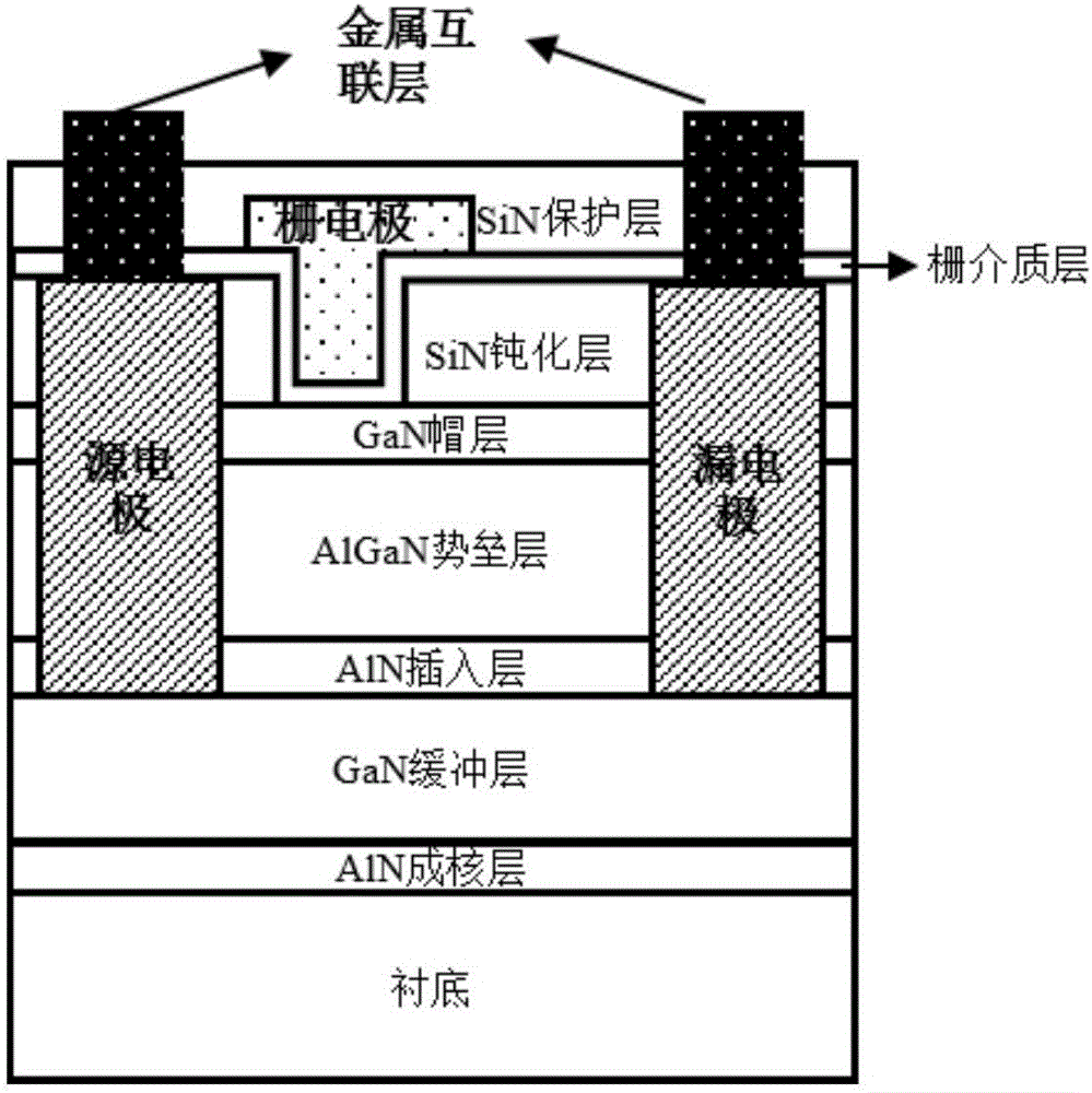
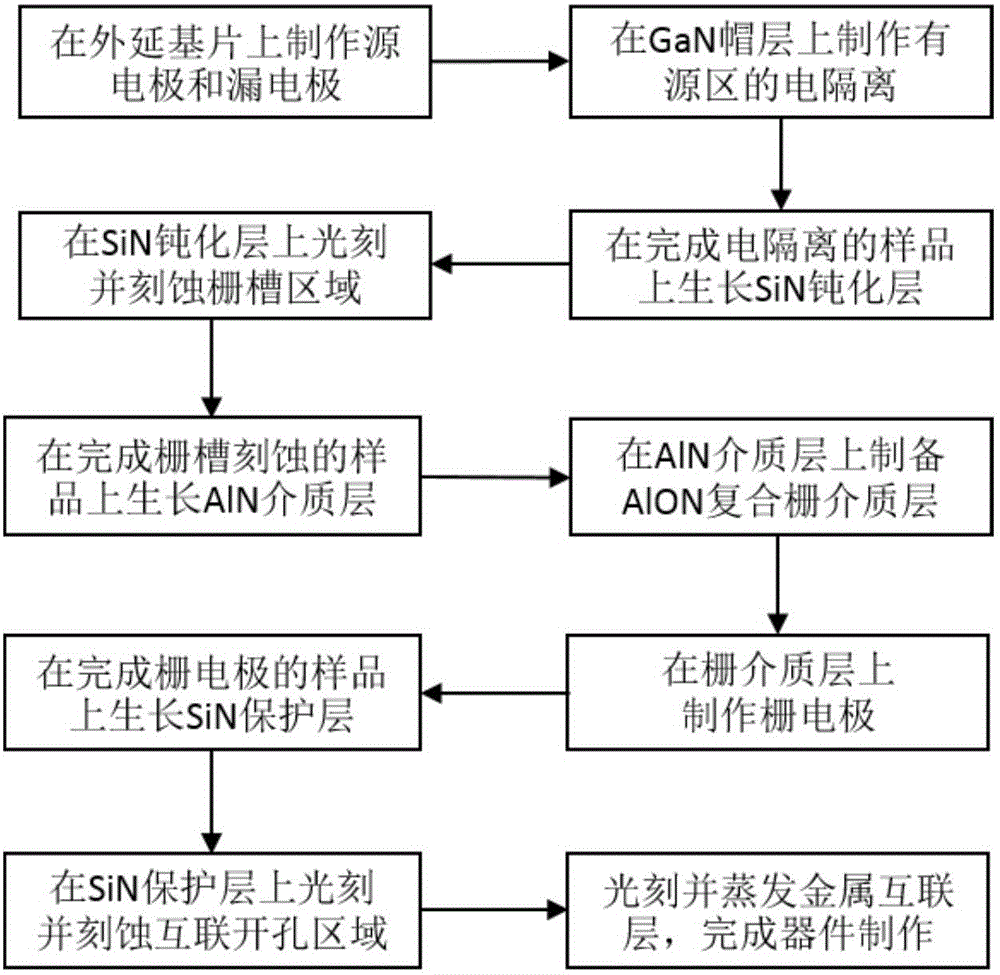
Fabrication method for transistor with composite gate dielectric GaN-based insulating gate and high electron mobility

A technology with high electron mobility and composite gate dielectric, applied in semiconductor/solid-state device manufacturing, circuits, electrical components, etc., can solve problems such as unstable oxygen substitution nitrogen, unstable threshold voltage, device performance degradation, etc., to achieve improved Effects of activity, reduction of interface charge, and improvement of compatibility

Active Publication Date: 2017-02-01
XIDIAN UNIV
View PDF5 Cites 15 Cited by
  • Summary
  • Abstract
  • Description
  • Claims
  • Application Information

AI Technical Summary

Problems solved by technology

However, the surface of nitride materials is very easily oxidized, forming unstable oxygen substitution nitrogen defects in the wurtzite nitride lattice
During the fabrication of insulated gate HEMT devices and the deposition of gate oxide dielectrics, the establishment of a low-quality interface oxide layer causes a high-density interface charge between the gate dielectric layer and the nitride barrier layer, and the charge / discharge effect of the interface state will cause serious threshold Reliability issues such as voltage instability, energy band modulation of interface charges and scattering of remote ionized impurities will cause device performance degradation such as threshold voltage negative drift, channel carrier mobility and transconductance reduction

Method used


Image

  • Fabrication method for transistor with composite gate dielectric GaN-based insulating gate and high electron mobility
  • Fabrication method for transistor with composite gate dielectric GaN-based insulating gate and high electron mobility

Examples


Embodiment 1

[0052] Embodiment 1, a GaN-based insulated gate high electron mobility transistor with an AlON composite gate dielectric layer thickness of 10 nm is fabricated on a sapphire substrate by thermal oxidation process.

[0053] Step 1, making source electrodes and drain electrodes on the GaN buffer layer of the epitaxial substrate.

[0054] 1a) Photoetching the source electrode region and the drain electrode region on the GaN cap layer:

[0055] First, bake the epitaxial substrate on a hot plate at 200°C for 5 minutes;

[0056] Then, apply and spin the peeling glue on the GaN cap layer, the thickness of the peeling glue is 0.35 μm, and bake the sample on a hot plate at 200 ° C for 5 minutes;

[0057] Next, apply and spin the photoresist on the stripping adhesive, the thickness of the coating is 0.77 μm, and bake the sample on a hot plate at 90°C for 1 min;

[0058] After that, put the sample that has been glued and glued into a photolithography machine to expose the photoresist i...

Embodiment 2

[0142] Embodiment 2, a GaN-based insulated gate high electron mobility transistor with an AlON compound gate dielectric layer thickness of 5 nm is fabricated on a SiC substrate by using a plasma-assisted oxidation process.

[0143] Step 1, making a source electrode and a drain electrode on the GaN buffer layer of the epitaxial substrate.

[0144] 1.1) Photoetching the source electrode region and the drain electrode region on the GaN cap layer:

[0145] The concrete realization of this step is identical with the step 1a) among the embodiment one;

[0146] 1.2) Evaporate the source and drain electrodes on the GaN cap layer within the source and drain electrode regions and on the photoresist outside the source and drain electrode regions:

[0147] The concrete realization of this step is identical with the step 1b) among the embodiment one;

[0148] 1.3) Put the ohmic metal evaporated and stripped sample into a rapid thermal annealing furnace for annealing treatment, so that th...

Embodiment 3

[0175] Embodiment 3, a GaN-based insulated gate high electron mobility transistor with an AlON compound gate dielectric layer thickness of 8 nm is fabricated on a Si substrate by using a plasma-assisted oxidation process.

[0176] Step A, making source electrodes and drain electrodes on the GaN buffer layer of the epitaxial substrate.

[0177] The specific implementation of this step is the same as step 1 in the first embodiment.

[0178] In step B, the electrical isolation area of ​​the active area is photolithographically etched on the GaN cap layer, and the electrical isolation of the active area of ​​the device is fabricated by using an ion implantation process.

[0179] The specific implementation of this step is the same as step 2 in the second embodiment.

[0180] In step C, a SiN passivation layer is grown on the GaN cap layer of the source electrode, the drain electrode and the active region by PECVD process.

[0181] The specific implementation of this step is the ...


PUM


Abstract

The invention discloses a fabrication method for a transistor with a composite gate dielectric GaN-based insulating gate and high electron mobility, mainly aims to solve the problem of low reliability a similar device. The fabrication method comprises the steps of manufacturing a source electrode, a drain electrode and an electric isolating region of an active region on an epitaxial wafer, and enabling an SiN passivation layer to be grown; photoetching and etching a gate slot region in the SiN passivation layer; enabling an AlN dielectric layer to be grown on the gate slot and the SiN passivation layer, and oxidizing the AlN dielectric layer into an AlON composite gate dielectric layer through thermal oxidization or plasma auxiliary oxidization process; manufacturing a gate electrode on the gate dielectric layer; enabling an SiN protection layer to be grown on the gate electrode and the gate dielectric layer out of the gate electrode region; photoetching and etching a metal interlinked open pore region in the SiN protection layer; and manufacturing a metal interlinking layer on the interlinked open pore region and the unopened and non-etched SiN protection layer to complete the manufacturing of the device. By adoption of the fabrication method, the interface characteristic of the device is improved, the reliability of the device is improved, and the device can be used as an efficient microwave power device.

Description

technical field [0001] The invention belongs to the technical field of semiconductor devices, in particular to a method for manufacturing high electron mobility transistors, which can be used for manufacturing high-frequency and high-power modules. Background technique [0002] Nitride semiconductor materials GaN, AlN, InN and their alloys are the third-generation wide-bandgap semiconductor materials after the first-generation elemental semiconductor materials Si, Ge and the second-generation compound semiconductor materials GaAs, InP, etc., which have a direct bandgap , Wide bandgap width, large continuous adjustable range, high breakdown field strength, fast saturated electron drift speed, high thermal conductivity, and good radiation resistance. With the improvement of technology and social development, the first and second generation semiconductor materials cannot meet the needs of higher frequency and higher power electronic devices. Electronic devices based on nitride ...

Claims


Application Information

Patent Timeline
Patent Type & Authority Applications(China)
IPC IPC(8): H01L21/335H01L21/285H01L21/02H01L29/423H01L29/51
CPCH01L21/02178H01L21/02274H01L21/0228H01L21/02337H01L29/42364H01L29/518H01L29/66462
Inventor 祝杰杰马晓华郝跃侯斌杨凌
Owner XIDIAN UNIV
Learn More