Substrate applying method, touch control display substrate and display apparatus

A technology for touch display substrates and display devices, applied in lamination devices, chemical instruments and methods, lamination auxiliary operations, etc., can solve problems such as easy generation of air bubbles, overflowing glue, and lack of glue, so as to reduce lamination air bubbles, Guaranteed optical performance and uniform thickness

Inactive Publication Date: 2015-01-28
HEFEI XINSHENG OPTOELECTRONICS TECH CO LTD +1
View PDF4 Cites 13 Cited by
  • Summary
  • Abstract
  • Description
  • Claims
  • Application Information

AI Technical Summary

Problems solved by technology

[0012] The purpose of the present invention is to solve the problem that the uniformity of the thickness of the adhesive layer is difficult to control when different functional units are attached in the display device in the prior art, and defects such as bubbles, overflowing glue, and lack of glue are prone to occur, resulting in a decrease in the optical performance of the display device. , providing a substrate bonding method, a touch display substrate and a display device

Method used


Image

  • Substrate applying method, touch control display substrate and display apparatus
  • Substrate applying method, touch control display substrate and display apparatus
  • Substrate applying method, touch control display substrate and display apparatus

Examples


Embodiment 1

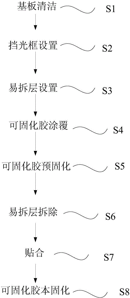
[0043] This embodiment provides a substrate bonding method, including the following steps:

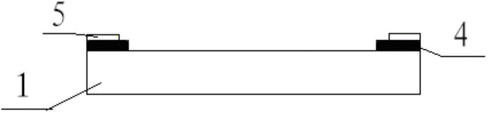
[0044] setting a light shielding frame in the peripheral area of ​​the surface to be bonded of the first substrate;

[0045] An easily detachable layer is set on the light blocking frame;

[0046] Coating curable glue on the surface to be bonded of the first substrate;

[0047] Pre-cure the curable glue;

[0048] The easy-detachable layer is removed, and the curable glue attached to the easy-detachable layer is removed at the same time.

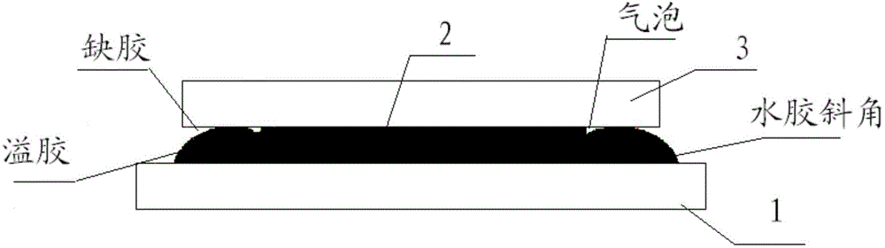
[0049] In the substrate laminating method, touch display substrate and display device of the present invention, since an easy-to-detachable layer is provided around the first substrate, and then the curable adhesive is applied, the curable adhesive is pre-cured and the easy-to-detachable layer is removed to enable The curable adhesive forms a special-shaped shape, the thickness of the curable adhesive layer is uniform, the surface is smooth, and th...

Embodiment 2

[0078] This embodiment provides a touch display substrate, and the touch display substrate is prepared by using the above-mentioned substrate bonding method.

[0079] Since the touch display substrate of this embodiment is prepared by the above-mentioned substrate bonding method, the optical performance of the touch display substrate is relatively good.

Embodiment 3

[0081] This embodiment provides a display device, which includes a touch display substrate.

[0082] Since the display device of this embodiment includes the above-mentioned touch display substrate, the optical performance of the display device is better.


PUM


Abstract

The invention provides a substrate applying method, a touch control display substrate and a display apparatus. The substrate applying method comprises the following steps: arranging detachable layers in the circumference of a first substrate, coating a light curable adhesive, pre-curing the light curable adhesive, and dismounting the detachable layers to make the light curable adhesive form a special shape. The method makes the thickness of the layer of the light curable adhesive uniform, the surface of the adhesive layer flattened and the slope angle of edges close to 90DEG, and also has the advantages of effective reduction of applying bubbles, control of the adhesive leaking and the adhesive spilling phenomena in edge areas during applying, and guaranteeing of the optical performances of the display apparatus.

Description

technical field [0001] The present invention relates to the field of display technology, and in particular, to a touch display substrate and a display device with a substrate bonding method. Background technique [0002] Electronic products with display functions such as mobile phones and computer televisions are increasingly widely used. During the manufacturing process, it is usually necessary to bond two substrates with functional layers, for example, bonding a touch screen substrate to a display substrate. [0003] There are generally two bonding processes. One is the frame glue bonding method. The frame glue used has a certain thickness. Taking the touch screen substrate bonded to the display substrate as an example, there will be a gap between the bonded touch screen and the display substrate. Filling the gap with air leads to insufficient bonding between the touch screen and the display substrate, which easily causes particles to infiltrate, and the optical performan...

Claims


Application Information

Patent Timeline
Patent Type & Authority Applications(China)
IPC IPC(8): B32B37/12
CPCB32B37/1284B32B38/18B32B2037/1253B32B2038/0076B32B2315/08B32B37/003G02F1/13338B32B2457/202B32B2457/208G02F1/133308G02F2202/28B32B37/12G02F1/133331B32B37/02B32B38/10
Inventor 罗鸿强许邹明范文金
Owner HEFEI XINSHENG OPTOELECTRONICS TECH CO LTD
Why Eureka
Try Eureka