Packaging structure and method of MEMS optical chip based on silicon-glass bonding

A technology for optical chips and packaging methods, applied in microstructure devices, processing microstructure devices, optics, etc., can solve problems such as wafer-level packaging difficulties of MEMS optical chips, improve reliability and stability, reduce costs, The effect of reducing packaging requirements

Active Publication Date: 2015-07-29
ANHUI CHINA SCI MW ELECTRONIC TECH CO LTD
View PDF8 Cites 8 Cited by
  • Summary
  • Abstract
  • Description
  • Claims
  • Application Information

AI Technical Summary

Problems solved by technology

[0007] In view of the shortcomings of the prior art described above, the purpose of the present invention is to provide a packaging structure and packaging method for MEMS optical chips based on silicon-glass bonding, which is used to solve the problem of wafer-level packaging of MEMS optical chips in the prior art. Ask a difficult question

Method used


Image

  • Packaging structure and method of MEMS optical chip based on silicon-glass bonding
  • Packaging structure and method of MEMS optical chip based on silicon-glass bonding
  • Packaging structure and method of MEMS optical chip based on silicon-glass bonding

Examples


Embodiment 1

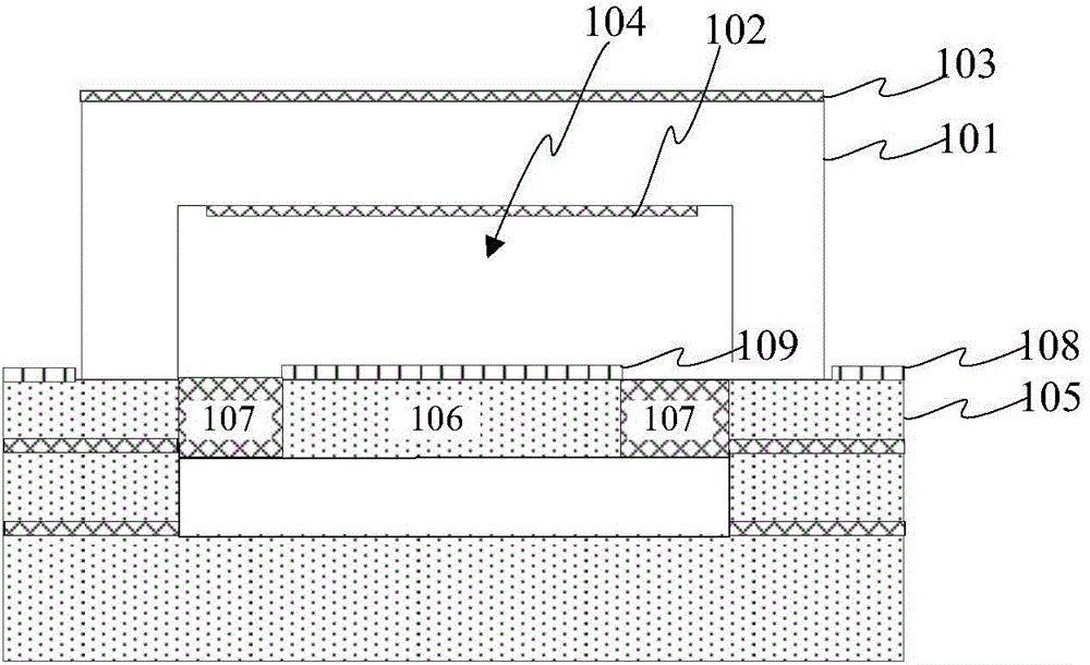
[0055] Such as figure 1 and Figure 3 ~ Figure 4 As shown, the present embodiment provides a packaging structure based on a silicon-glass bonding MEMS optical chip, including:

[0056] The first part comprises an optical glass 101, its upper surface is plated with an optical anti-reflection film 103, and a cavity 104 is formed on the lower surface to provide an airtight micromirror movement space for the MEMS optical chip. The upper surface of the cavity 104 Meet the requirements of optical surface finish, and coated with the lower optical anti-reflection film 102;

[0057] The second component includes a MEMS optical chip, and the MEMS optical chip can realize the manipulation of the optical signal under the action of the MEMS driver;

[0058] The first component and the second component realize wafer-level bonding through silicon-glass bonding, and form an independent sealed cavity for each MEMS optical chip. Specifically, the MEMS optical chip includes a bulk silicon su...

Embodiment 2

[0077] Such as figure 1 and Figure 3 ~ Figure 4 As shown, the present embodiment provides a packaging structure of MEMS optical chips based on silicon-glass bonding, and its basic structure is as described in Embodiment 1, wherein the optical glass 101 having a cavity 104 is composed of two optical Made of glass bonding, it includes a first optical glass 102 and a second optical glass 101 with through holes processed at positions corresponding to the MEMS optical chip, and then the optical glass with a cavity 104 is formed by bonding these two optical glasses.

[0078] Such as Figure 6a ~ Figure 6g As shown, this embodiment also provides a method for packaging MEMS optical chips based on silicon-glass bonding, the basic steps of which are as in Embodiment 1, wherein, as Figure 6a ~ Figure 6c As shown, step 1) includes steps:

[0079] Such as Figure 6b As shown, at first step 1-1) is carried out, the first optical glass 102 is provided, and a through hole is processed ...

Embodiment 3

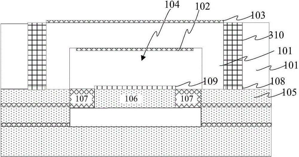
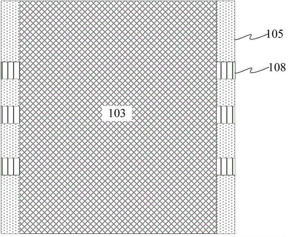
[0084] Such as Figure 2 ~ Figure 4 As shown, the present embodiment provides a packaging structure based on a silicon-glass bonding MEMS optical chip, and its basic structure is as in Embodiment 1, wherein, the TGV structure 310 is prefabricated in the optical glass, and its position is the same as that of the MEMS optical chip. The positions of the electrode pads 108 of the chips correspond one by one. After the silicon-glass bonding of the first component and the second component, the TGV structure 310 directly leads the electrode pads 108 of the MEMS optical chip to the upper surface of the optical glass.

[0085] Such as Figure 7a ~ Figure 7e As shown, this embodiment also provides a method for packaging MEMS optical chips based on silicon-glass bonding, the basic steps of which are as in Embodiment 1, wherein, as Figure 7b As shown, step 1) also includes: the step of prefabricating a TGV structure 310 on the optical glass, the position of the TGV structure 310 corresp...


PUM


Abstract

The invention provides a packaging structure and method of an MEMS optical chip based on silicon-glass bonding. The packaging structure comprises a first part and a second part, wherein the first part comprises optical glass of which the upper surface is coated with an upper optical antireflection film and while the lower surface is provided with a cavity; the upper surface of the cavity meets the requirement on smoothness of an optical surface, and a lower optical antireflection film is plated; the second part comprises the MEMS optical chips; the first part and the second part are subjected to silicon-glass bonding to achieve chip-stage bonding, and an independent sealing cavity is formed for each MEMS optical chip. With the adoption of the structure and the method, the chip-stage packaging requirement can be achieved; the reliability and stability of the chip can be improved; the electric performance, mechanical performance and optical performance for application of the optical chip can be ensured; in addition, the comprehensive level superior to that of other packaging technologies is brought; the packaging cost can be reduced; the packaging efficiency can be increased; the light loss can be decreased; the structure and the method have a wide application prospect in the packaging of optical communication devices and optical sensors.

Description

technical field [0001] The invention belongs to the fields of micro-electromechanical systems (MEMS), optical communications, optical sensors, spectral analysis, and adjustable lasers, and in particular relates to a packaging structure and packaging method for MEMS optical chips based on silicon-glass bonding. Background technique [0002] MEMS chips with tunable optical functions are key devices in intelligent optical communication or fiber optic sensing, and common ones include optical attenuators (VOA), optical switches, optical tunable filters, etc. MEMS optical chips generally include movable optical micro-mirrors and corresponding micro-drivers and micro-structures, which have extremely high requirements for environmental cleanliness. Usually, they can only be exposed to the air in a 1000-level purification environment, and they are also relatively sensitive to air humidity. Sensitive, many MEMS optical chips cannot be practically applied due to unsolved packaging prob...

Claims


Application Information

Patent Timeline
Patent Type & Authority Applications(China)
IPC IPC(8): B81B7/02B81C3/00G02B26/00
Inventor 吴亚明翟雷应徐静沈时强
Owner ANHUI CHINA SCI MW ELECTRONIC TECH CO LTD
Why Eureka
Try Eureka