

Method for reducing photoresist figure linewidth roughness
A line width roughness, photoresist technology
- Summary
- Abstract
- Description
- Claims
- Application Information
AI Technical Summary
Problems solved by technology
Method used
Image

Examples
no. 1 example
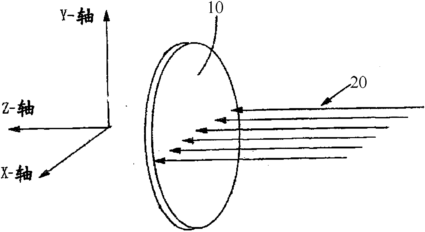
[0037] The method for reducing the line width roughness of the photoresist pattern provided by the present invention includes: as figure 1 As shown, the substrate 10 with a photoresist pattern (not shown) on the surface is placed in a vacuum chamber (not shown); the photoresist pattern is ion-implanted with a ribbon ion beam 20 to reduce the photoresist pattern. Low-frequency linewidth roughness for glue patterns.
[0038] The so-called ribbon ion beam 20 refers to: the cross section of the ion beam 20 (the cross section perpendicular to the Z-axis direction) is rectangular, and the size of the ion beam 20 in the X-axis direction is much larger than the size in the Y-axis direction, Alternatively, the size of the ion beam 20 is much smaller in the direction of the X-axis than the Y-axis, wherein the Z-axis is perpendicular to the substrate 10, both the X-axis and the Y-axis are perpendicular to the Z-axis, and the X-axis is perpendicular to the Y-axis. In other words, the rib...
no. 2 example
[0057] The difference between the second embodiment and the first embodiment is that: in the first plasma processing step of the second embodiment, the first radio frequency power supply for forming the first plasma is turned on intermittently; While in the first plasma processing step of the first embodiment, the first radio frequency power source for forming the first plasma is continuously turned on.
[0058] Research has found that the second embodiment can bring the following further beneficial effects on the basis of the first embodiment: as mentioned above, when the substrate is exposed to the first plasma environment, the surface of the photoresist pattern will form A graphite-like layer, and when the thickness of the graphite-like layer is larger, the line width roughness of the photoresist pattern will be increased, when the first radio frequency power supply for forming the first plasma is turned on intermittently , the thickness of the graphitic layer can be reduce...
no. 3 example
[0064] The difference between the third embodiment and the first embodiment is that in the third embodiment, in addition to the first plasma treatment after the ion implantation, it also includes: exposing the substrate to 2 In the second plasma environment formed by the gas, the photoresist pattern is subjected to the second plasma treatment. In this embodiment, the first plasma treatment can be performed first, then the second plasma treatment, and then chemical vapor deposition, or the second plasma treatment can be performed first, then the first plasma treatment, and then chemical vapor deposition. vapor deposition.
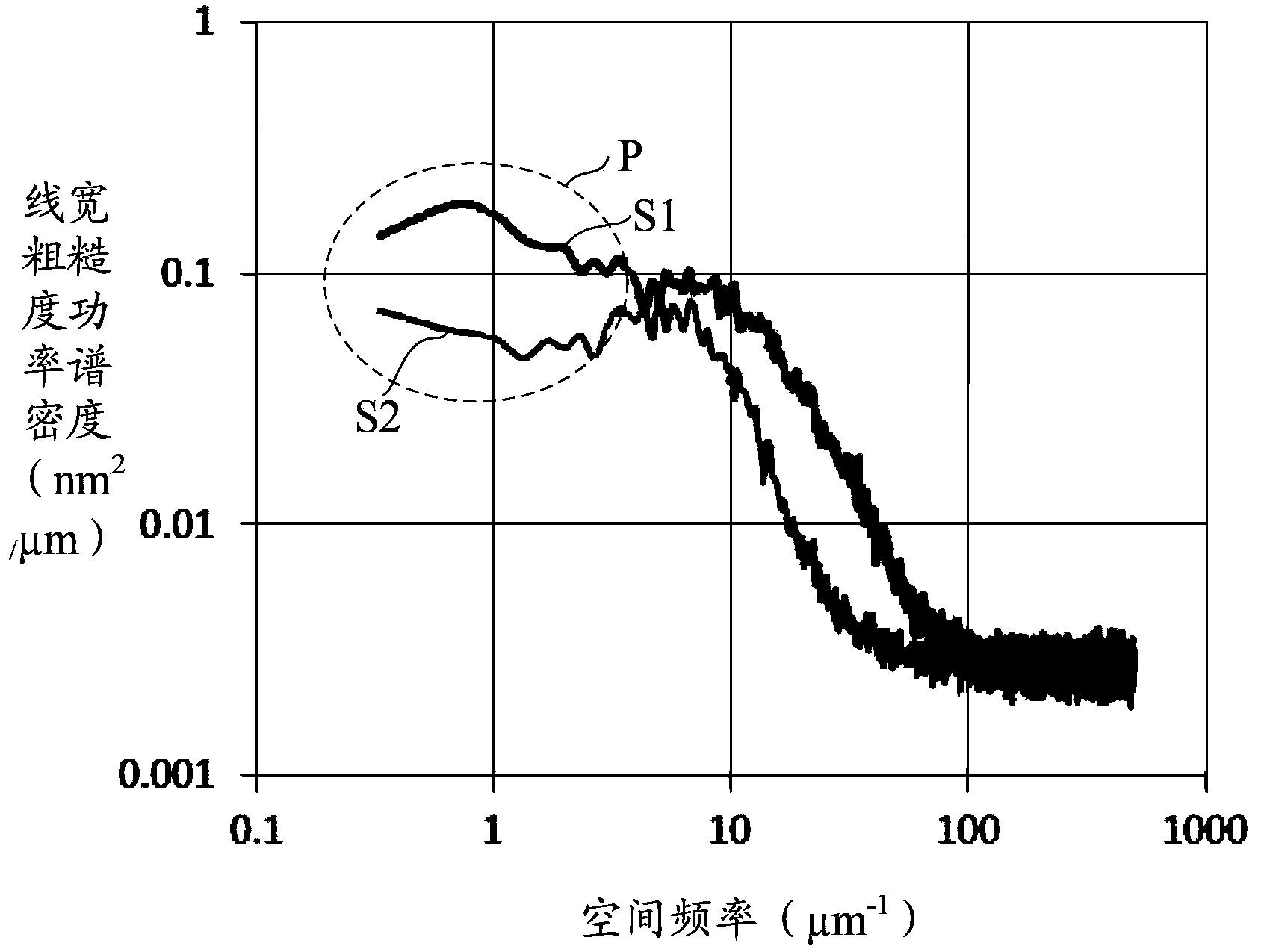
[0065] Research has found that the third embodiment can bring the following further beneficial effects on the basis of the first embodiment: the C-O bond in the photoresist pattern is closely related to the high-frequency line width roughness of the photoresist pattern, when the light When there are fewer C-O bonds in the resist pattern, the high-frequency ...
PUM
 Abstract
Description
Claims
Application Information