Semiconductor device forming method

A semiconductor and device technology, applied in the field of semiconductor device formation, can solve problems such as reducing the yield of semiconductor devices and affecting the performance of semiconductor devices, and achieve the effects of improving electrical performance, increasing low-frequency line width roughness, and improving morphology

Active Publication Date: 2016-11-23
SEMICON MFG INT (SHANGHAI) CORP
View PDF5 Cites 8 Cited by
  • Summary
  • Abstract
  • Description
  • Claims
  • Application Information

AI Technical Summary

Problems solved by technology

[0004] In the process of gradually shrinking line width, the problems caused by LWR will exceed the allowable error of CD in se...

Method used


Image

  • Semiconductor device forming method
  • Semiconductor device forming method
  • Semiconductor device forming method

Examples


Embodiment Construction

[0031] It can be seen from the background art that in the process of forming a semiconductor device, the line width roughness of the photoresist layer is one of the important factors affecting the performance and yield of the semiconductor device.

[0032] After research, it is found that in addition to the line width roughness of the photoresist layer, the "roughness profile" of the photoresist layer can also include line edge roughness, and short, medium, and long distance line width roughness changes, and its parameters correspond to It exhibits different length scales in the direction along which the line width changes. In addition to the absolute value of line width roughness or line edge roughness, the length scale at which this variation occurs is also one of the keys to semiconductor device fabrication.

[0033] The long-distance line width roughness change of the photoresist layer corresponds to the low frequency (Low Frequency) line width roughness; the middle distan...


PUM


Abstract

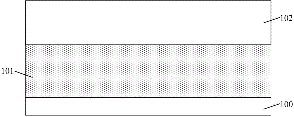
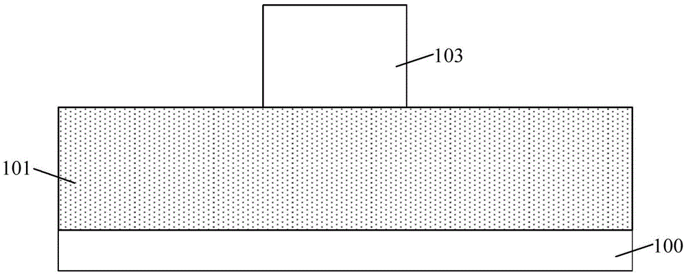
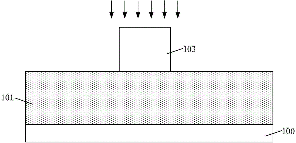
A semiconductor device forming method includes providing a to-be-etched layer whose surface is provided with an initial photoresist film; performing photoetching on the initial photoresist film so as to form a photoresist layer having a first line width roughness; performing side wall backflow repair treatment on the photoresist layer and enabling the photoresist layer subjected to the side wall backflow repair treatment to have a second line width roughness smaller than the first line width roughness; forming a solidification layer on the top part surface and the side wall surface of the photoresist layer after the side wall backflow repair treatment; and forming a size repair layer on the solidification layer. According to the invention, the line width roughness of a mask pattern of the to-be-etched layer is reduced, the size of the mask pattern is consistent to a preset target size, and the performance and yield of a formed semiconductor device are improved.

Description

technical field [0001] The invention relates to the technical field of semiconductor manufacturing, in particular to a method for forming a semiconductor device. Background technique [0002] The process flow of semiconductor manufacturing technology includes two important process steps of photolithography and etching. In the photolithography process, the photoresist is firstly spin-coated on the substrate, and then the spin-coated photoresist is soft-dried to make it a solid film; forming a desired photoresist pattern in the resist; then, using the photoresist pattern as a mask, an etching step is performed on the substrate, so that the photoresist pattern is transferred into the substrate. After the etching of the substrate is completed, the photoresist is no longer needed as a protective layer and can be removed. [0003] With the advancement of semiconductor manufacturing technology, in order to achieve faster computing speed, larger data storage capacity and more func...

Claims


Application Information

Patent Timeline
IPC IPC(8): H01L21/027
CPCH01L21/0273H01L21/0274
Inventor 张海洋张城龙
Owner SEMICON MFG INT (SHANGHAI) CORP
Why Eureka
Try Eureka