

Transparent conducting film
A technology of transparent conductive film and conductive layer, applied to conductive layers, circuits, electrical components and other directions on insulating carriers, can solve the problems of waste of precious metals, weak conductivity, and poor conductivity, and achieve the effect of enhancing conductivity.
- Summary
- Abstract
- Description
- Claims
- Application Information
AI Technical Summary
Problems solved by technology
Method used
Image


Examples
Embodiment 1
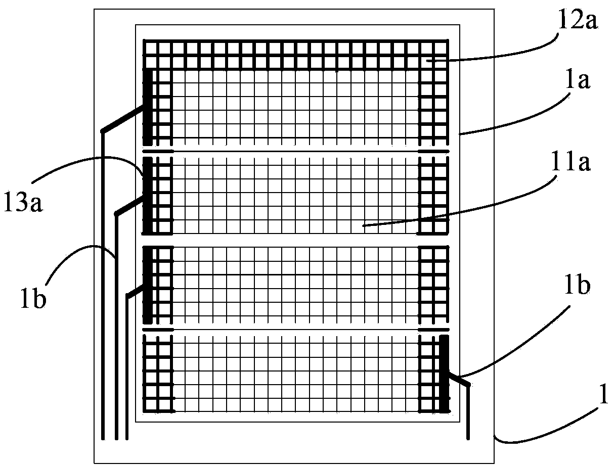
[0040] Such as Figure 1-3 As shown, the embodiment of the present invention provides a transparent conductive film, and the transparent conductive film includes a substrate 1, a first conductive layer 1a, and a first lead electrode 1b;
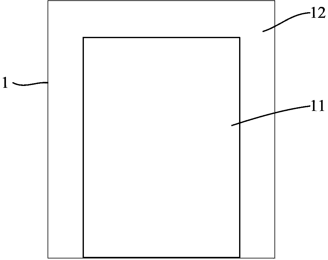
[0041] A sensing area 11 and a lead area 12 located at the edge of the sensing area 11 are provided on one side of the substrate 1;
[0042] The first conductive layer 1a includes a grid-shaped first conductive pattern, the first conductive pattern is arranged in the sensing area 11 and the lead area 12 and connected to each other, and the first conductive pattern is composed of conductive lines;
[0043] The first lead electrode 1b is arranged in the lead area 12, and the first lead electrode 1b is electrically connected to the first conductive layer 1a;
[0044] Wherein, the conductive line width of the first conductive pattern 11a located in the sensing area is smaller than the conductive line width of the first conductive pattern 12a loc...
Embodiment 3
[0052] Another embodiment is as follows, the conductive film is a single-sided double-layer structure, see Figure 6 , Figure 7 , the second conductive layer 2a is arranged on the first conductive layer 1a, and an insulating layer 30 is arranged between the first conductive layer 1a and the second conductive layer 2a, and the projection of the second conductive layer 2a is located in the sensing area and toward the lead wire The second lead electrode 2b is arranged on the insulating layer 30, and the projection of the second lead electrode 2b is located in the lead area and is electrically connected with the second conductive pattern 22a' projected in the lead area; the second conductive pattern 22a' projected in the sensing area The conductive line width of the pattern 21a' is smaller than the conductive line width of the second conductive pattern 22a' projected on the lead area. The conductivity between the second conductive layer and the second lead electrode is increased...
Embodiment 4
[0056] Such as Figure 8 As shown, there is a first base layer 10 between the first conductive layer 1a and the substrate 1, grid-like grooves are provided on the first base layer 10, and first conductive patterns are embedded in the grid-like grooves.
PUM
 Abstract
Description
Claims
Application Information