
OLED display panel

A technology of light-emitting diodes and display panels, which is applied to static indicators, instruments, electrical components, etc., can solve the problems of increasing the burden of organic light-emitting diode display panels, and achieve the effect of large openings and increased pixel density

Inactive Publication Date: 2015-02-11
HONG FU JIN PRECISION IND (SHENZHEN) CO LTD +1
View PDF4 Cites 9 Cited by
  • Summary
  • Abstract
  • Description
  • Claims
  • Application Information

AI Technical Summary

Problems solved by technology

However, when a higher pixel density (pixels per inch) is required, the sub-pixels are arranged more closely, which increases the burden on the fabrication of the existing OLED display panel.

Method used


Image

  • OLED display panel
  • OLED display panel
  • OLED display panel

Examples


Embodiment Construction

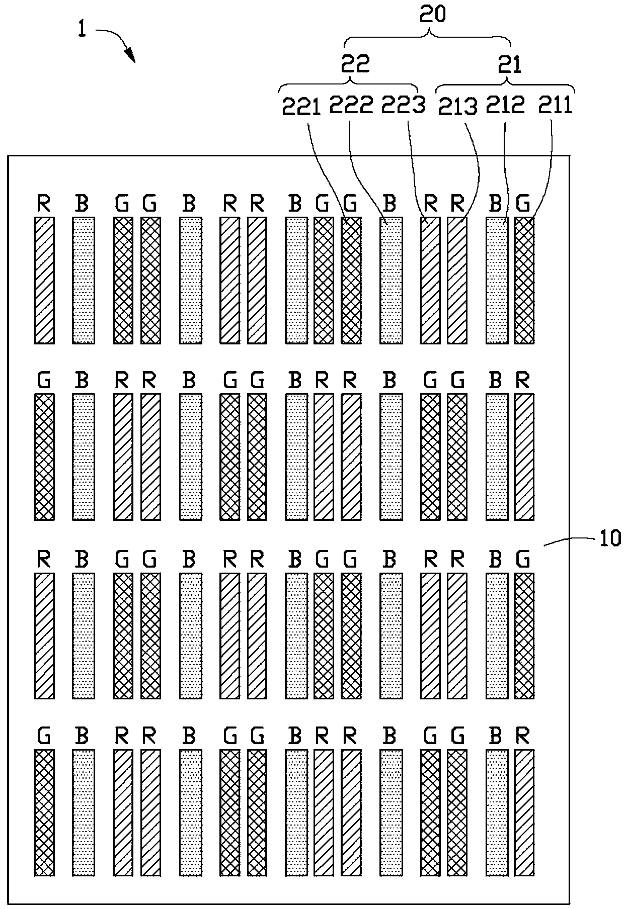
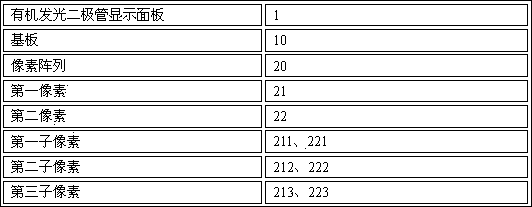
[0012] see figure 2 , shows the organic light emitting diode display panel 1 of the first embodiment of the invention. The OLED display panel 1 includes a substrate 10 and a pixel array 20 formed on the substrate 10 . The pixel array 20 is composed of a plurality of first pixels 21 and second pixels 22 . Each first pixel 21 includes a first sub-pixel 211, a second sub-pixel 212, and a third sub-pixel 213 arranged in parallel and at intervals, and each second pixel 22 includes a first sub-pixel arranged in parallel and at intervals 221 , a second sub-pixel 222 and a third sub-pixel 223 . In this embodiment, the first sub-pixel 211 in the first pixel 21 is a green sub-pixel, the second sub-pixel 212 is a blue sub-pixel, and the third sub-pixel 213 is a red sub-pixel; The first sub-pixel 221 is a green sub-pixel, the second sub-pixel 222 is a blue sub-pixel, and the third sub-pixel 223 is a red sub-pixel.

[0013] The first pixel 21 and the second pixel 22 in the same row ar...


PUM


Abstract

An OLED display panel includes a plurality of spaced first pixels and a plurality of spaced second pixels arranged in rows and columns. Each of the first pixels includes a first sub-pixel, a second sub-pixel and a third sub-pixel. The first sub-pixel, the second sub-pixel and the third sub-pixel of each first pixel are substantially parallel to and spaced from each other. Each of the second pixels includes a first sub-pixel, a second sub-pixel and a third sub-pixel. The first sub-pixel, the second sub-pixel and the third sub-pixel of each second pixel are substantially parallel to and spaced from each other. The first pixels and the second pixels are arranged in alternate pattern in one row, and the first pixels and the second pixels are arranged in alternate pattern in one column

Description

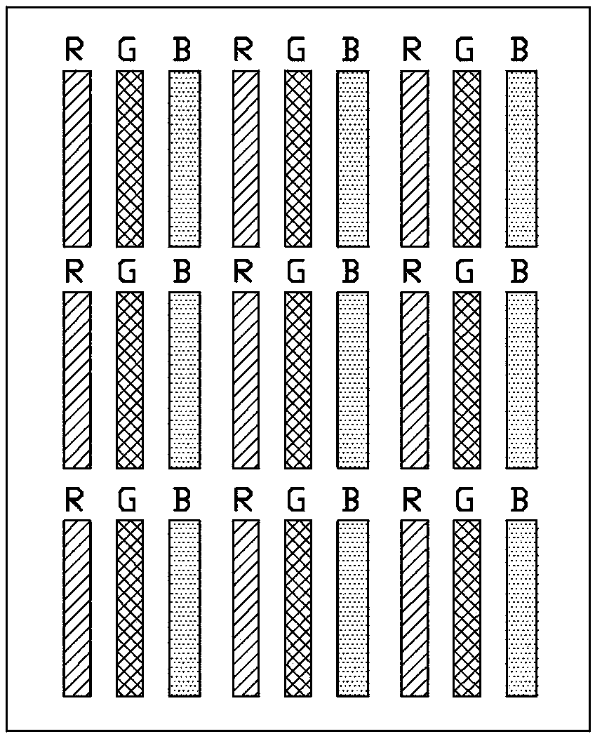
technical field [0001] The invention relates to an organic light emitting diode display panel. Background technique [0002] As an emerging light source, organic light-emitting diodes are the development direction of next-generation displays. OLED panels are made up of multiple pixels. Such as figure 1 As shown, each pixel contains three sub-pixels of red, green and blue to produce a color image. However, when a higher pixel density (pixels per inch) is required, the sub-pixels are arranged more closely, which increases the burden on the fabrication of the existing OLED display panel. Contents of the invention [0003] Therefore, it is necessary to provide an OLED display panel with higher pixel density. [0004] An organic light emitting diode display panel, including a plurality of first pixels and second pixels arranged in an array, each first pixel includes first sub-pixels, second sub-pixels and third sub-pixels arranged in parallel and at intervals, each first pi...

Claims


Application Information

Patent Timeline
Patent Type & Authority Applications(China)
IPC IPC(8): H01L27/32
CPCG09G3/3225G09G3/3208G09G2300/0452H10K59/353
Inventor 黄俊杰
Owner HONG FU JIN PRECISION IND (SHENZHEN) CO LTD
Learn More