A kind of preparation method of tunneling field effect transistor

A tunneling field effect and transistor technology, which is applied in semiconductor/solid-state device manufacturing, semiconductor devices, electrical components, etc., can solve problems such as potential crosstalk and insufficient substrate resistance, and achieve the effect of avoiding the increase of leakage current

Active Publication Date: 2017-12-01
PEKING UNIV
View PDF7 Cites 0 Cited by
  • Summary
  • Abstract
  • Description
  • Claims
  • Application Information

AI Technical Summary

Problems solved by technology

When TFET devices form a complex circuit, NTFET and PTFET share the same substrate, because the substrate resistance is usually not high enough, resulting in the P of different TFET devices + regions can be connected to each other through the substrate, while the P of different TFET devices in circuit applications + There may be differences in the potential of the region, so the lightly doped substrate will cause potential crosstalk, which is a big problem in a circuit composed of TFET devices, and a method for effectively isolating each TFET device is needed

Method used


Image

  • A kind of preparation method of tunneling field effect transistor
  • A kind of preparation method of tunneling field effect transistor
  • A kind of preparation method of tunneling field effect transistor

Examples


Embodiment Construction

[0035] The present invention will be further illustrated by examples below. It should be noted that the purpose of publishing the embodiments is to help further understand the present invention, but those skilled in the art can understand that various substitutions and modifications are possible without departing from the spirit and scope of the present invention and the appended claims. of. Therefore, the present invention should not be limited to the content disclosed in the embodiments, and the scope of protection claimed by the present invention is subject to the scope defined by the claims.

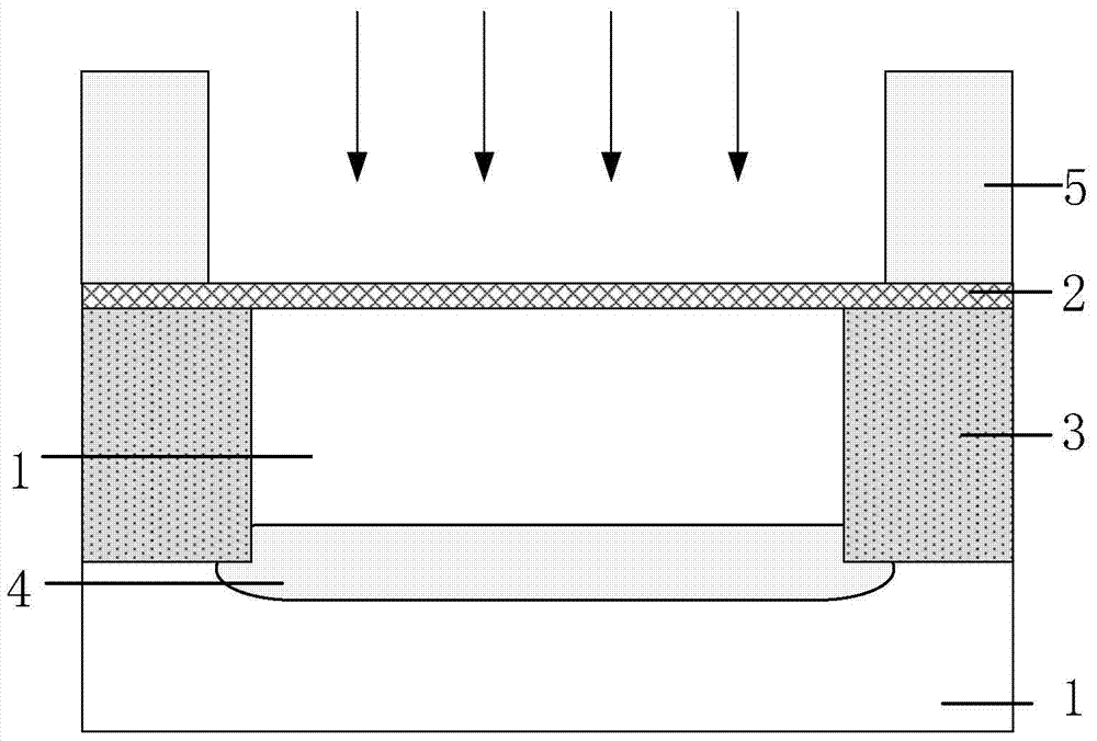
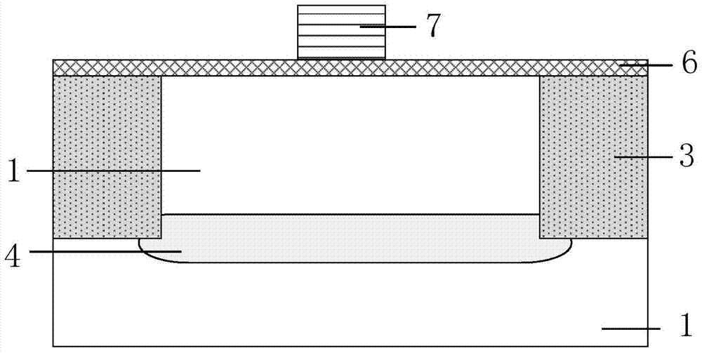
[0036] A specific example of the preparation method of the present invention includes Figure 1 to Figure 6 Process steps shown:

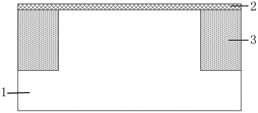
[0037] 1. The doping concentration of the substrate is lightly doped and the crystal orientation is A layer of silicon dioxide 2 is initially thermally oxidized on the bulk silicon substrate 1 with a thickness of about 10 nm, and a layer of silicon nitride ...


PUM


Abstract

The invention discloses a production method of a tunneling field-effect transistor and belongs to the field of CMOS (complementary metal-oxide-semiconductor transistor) ULSI (ultra-large scale integrated circuits) and their field-effect transistor logic devices. According to the production method, a p-type silicon wafer of relative high impedance is used as a trench region and a body region of a TFET (tunneling field-effect transistor) device, a mask for injection of an N<-> region is added on basis of the standard CMOS-IC process, the N<-> region injected deep in a trench, device isolation is achieved for the TFET in circuit application, and device performances and device area are unaffected.

Description

Technical field [0001] The invention belongs to the field of field effect transistor logic devices and circuits in CMOS ultra-large integrated circuits (ULSI), and specifically relates to a method for isolating tunneling field effect transistors (TFET). Background technique [0002] As the size of the MOSFET enters the nanometer scale, the negative effects such as the short channel effect of the device have become more serious, and the off-state leakage current of the device has been increasing. At the same time, because the sub-threshold slope of the traditional MOSFET is limited by the thermoelectric potential, it cannot decrease simultaneously with the shrinking of the device size. There is a theoretical limit of 60mV / dec, which makes the leakage current further increase with the shrinking of the power supply voltage. Increased device power consumption. The power consumption problem has now become one of the most severe problems restricting the scaling of devices. In the fie...

Claims


Application Information

Patent Timeline
Patent Type & Authority Patents(China)
IPC IPC(8): H01L21/336
CPCH01L21/761H01L29/1033H01L29/66477
Inventor 黄如黄芊芊廖怀林叶乐吴春蕾朱昊王阳元
Owner PEKING UNIV
Why Eureka
Try Eureka