

A kind of preparation method of light-emitting element
A light-emitting element and atmosphere technology, applied in electrical components, semiconductor devices, circuits, etc., can solve the problems of carrier leakage, non-radiative recombination centers, increase, and high defect density of epitaxial structures, so as to improve wavelength uniformity and warpage , the effect of enhancing the effect
- Summary
- Abstract
- Description
- Claims
- Application Information
AI Technical Summary
Problems solved by technology
Method used
Image

Examples
Embodiment 1
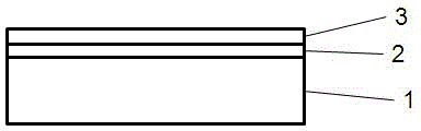
[0036] attached Figure 1~4The first preferred embodiment of the present invention is disclosed. A method for preparing a light-emitting element. First, a substrate 1 is provided, which can be sapphire, silicon, silicon carbide, etc. Here, a sapphire flat substrate is preferred, and it is placed in a PVD chamber, and the temperature of the chamber is adjusted to 300-600°C , the pressure is 2-10mtorr, and the AlN film layer 2 with a thickness of 10-350nm is deposited by PVD method. ℃, through the metal source, NH3, H2 epitaxial growth of Al x Ga 1-x N (0≤xfigure 1 shows the growth of Al x Ga 1-x Schematic diagram of the structure after N (0≤x<1) layers.
[0037] in Al x Ga 1-x After the N (0≤xx Ga 1-x N (0≤x figure 2 shown. Figure 4 For the change over time during the preparation of the light-emitting element in this implementation, NH 3 , metal source, H 2 Schematic diagram of the relationship between valve open (on) / off (off) state and temperature change, which sh...
Embodiment 2
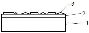
[0041] See attached Figure 5 and 6 , the difference between this embodiment and embodiment 1 is: the annealing process is all H 2 Ambience, i.e. in H 2 Turn off the metal source and NH3 while still connected, and change the chamber temperature from Al to 500s x Ga 1-x The growth temperature (400-600) of the N (0≤x2 Etching strength is higher than that of NH 3 more obvious, so when the temperature rises, the Al x Ga 1-x N (0≤x2 For the formed Al x Ga 1-x N layer 3 is etched, when part thickness is thinner Al x Ga 1-x When the N layer 3 is etched to expose the underlying AlN film layer 2, H 2 Continue to etch the AlN film layer 2 to form an over-etched uneven shape on the surface, then when the GaN layer 4 is subsequently deposited, the growth rate of the GaN layer 4 on the surface of the over-etched AlN film layer is lower than that of the island-like or irregular shape after annealing. Al x Ga 1-x The growth rate of the GaN layer 4 on the surface of the N layer 3...
Embodiment 3
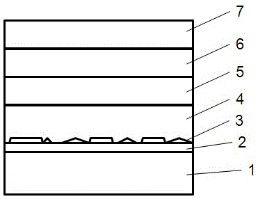
[0043] Please see attached Figure 7-9 , The difference between this embodiment and Embodiment 1 is that a patterned substrate 1 is used, preferably a convex patterned substrate, which can be a platform-shaped, tapered or cylindrical, etc. prepared by wet etching or dry etching. Raised periodic pattern. First, put the patterned substrate 1 into the PVD chamber, deposit the AlN film layer 2, and then transfer the substrate coated with the AlN film layer 2 into the CVD chamber, and epitaxially grow Al x Ga 1-x N (0≤x Figure 7 shown. Then use H 2 Vibe and NH 3 Combined atmosphere for annealing treatment, the specific annealing method and conditions can refer to embodiment 1, using H 2 The strong etching performance and high temperature conditions have a great influence on the Al x Ga 1-x N layer 3 is etched and recrystallized, because the Al on the sidewall and top of the pattern x Ga 1-x The thickness of the N layer is higher than that of Al x Ga 1-x The N layer is re...
PUM
| Property | Measurement | Unit |
|---|---|---|
| thickness | aaaaa | aaaaa |
| thickness | aaaaa | aaaaa |
Abstract
Description
Claims
Application Information