Packaging structure for rewiring of packaged two-sided BUMP chip and manufacturing method of packaging structure

A packaging structure and rewiring technology, applied in semiconductor/solid-state device manufacturing, electrical components, electrical solid-state devices, etc., can solve the problems of top-layer chip limitation, overall package size thick, top-layer chip flip position cannot exceed the bottom chip, etc. Achieve the effect of shortening the path, improving the quality, chip size and I/O location flexibility

Active Publication Date: 2015-03-11
JCET GROUP CO LTD
View PDF11 Cites 10 Cited by
  • Summary
  • Abstract
  • Description
  • Claims
  • Application Information

AI Technical Summary

Problems solved by technology

[0007] The first is a common stacked product. This structure has restrictions on the top chip, not only the size of the chip, but also the use of bonding wires to interconnect the chips;
[0008] The second is the product of direct TSV stacking. In this method, the flip position of the top chip cannot exceed the size of the bottom chip;
[0009] The third is to use POP technology to stack packages such as Figure 12 , the overall size of the package will be relatively thick due to the top-level packaged substrate in this way of stacking

Method used


Image

  • Packaging structure for rewiring of packaged two-sided BUMP chip and manufacturing method of packaging structure
  • Packaging structure for rewiring of packaged two-sided BUMP chip and manufacturing method of packaging structure
  • Packaging structure for rewiring of packaged two-sided BUMP chip and manufacturing method of packaging structure

Examples


Embodiment Construction

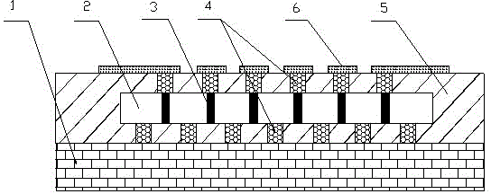
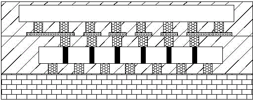
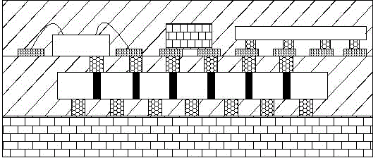
[0044] See figure 1 , The present invention relates to a double-sided BUMP chip encapsulation and rewiring packaging structure, which includes a substrate 1 and a chip 2, on which a plurality of through holes 3 are processed through a silicon via (TSV) process, and the chip 2 Metal bumps (BUMP) 4 are provided on the front and back sides of the chip 2 and the chip 2 is soldered to the front surface of the substrate 1 through the bump 4 on the front side. The bumps 4 on the front and back sides of the chip 2 and the chip 2 are enclosed Plastic compound 5, the front surface of the plastic compound 5 is flush with the top of the bump 4 on the back of the chip 2, and a metal circuit layer 6 is provided on the front surface of the plastic compound 5, and the metal circuit layer 6 is aligned with the bumps on the back of the chip 2. Block 4 is connected.

[0045] The metal circuit layer 6 realizes rewiring after encapsulation, and provides electrical connections for subsequent chips an...


PUM


Abstract

The invention relates to a packaging structure for rewiring of a packaged two-sided BUMP chip and a manufacturing method of the packaging structure. The packaging structure comprises a base plate (1) and a chip (2). The packaging structure is characterized in that a plurality of through holes (3) are formed in the chip (2); bumps (4) are arranged on the front side and the back side of the chip (2); the chip (2) is welded on the front side of the base plate (1) through the bump (4) on the front side; the peripheries of the chip and the bumps (4) on the front side and the back side of the chip (2) are wrapped with a plastic packaging material (5); the front side of the plastic packaging material (5) is flush with the top of the bump (4) on the back side of the chip (2); a metal circuit layer (6) is arranged on the front side of the plastic packaging material (5); the metal circuit layer (6) is connected with the bumps (4) on the back side of the chip (2). By adopting the packaging structure, the flexibility of the mounting mode of a top-layer chip is improved, the height of a product is reduced, the signal transmission route is shortened, and the signal quality is improved.

Description

Technical field [0001] The invention relates to a double-sided BUMP (bump) chip encapsulation and rewiring packaging structure and a manufacturing method thereof. It belongs to the field of electronic packaging technology. Background technique [0002] There are currently three stacking methods for products stacked in electronic packaging: [0003] The first type is a normal stacked product. Its structure is to directly stack the chips on top of the chips, then wire them, and then encapsulate them. Picture 10 ; [0004] The second type is a direct TSV stacking product. Its structure is to use FC process stacking chips on the chip after TSV. Picture 11 ; [0005] The third is to use POP technology to stack packaging on top of the plastic package such as Picture 12 . [0006] The above method of stacking products has the following shortcomings: [0007] The first type is a normal stacked product. This structure has limitations on the top chip, not only the chip size, but also can only ...

Claims


Application Information

Patent Timeline
Patent Type & Authority Applications(China)
IPC IPC(8): H01L23/488H01L21/60
CPCH01L2224/48091H01L2924/00014
Inventor 杨志赵励强唐悦王新缪富军
Owner JCET GROUP CO LTD
Why Eureka
Try Eureka