Packaging structure adopting flexible substrate and TSV chip and manufacturing method of packaging structure

A technology of flexible substrates and packaging structures, applied in semiconductor/solid-state device manufacturing, electrical components, electrical solid-state devices, etc., can solve problems such as wire-bonded chips, and achieve the effect of improving quality, improving product performance, and shortening the path

Inactive Publication Date: 2019-07-19
JCET GROUP CO LTD
View PDF4 Cites 0 Cited by
  • Summary
  • Abstract
  • Description
  • Claims
  • Application Information

AI Technical Summary

Problems solved by technology

This structure has restrictions on the top chip, which can only be a bonded chip;

Method used


Image

  • Packaging structure adopting flexible substrate and TSV chip and manufacturing method of packaging structure
  • Packaging structure adopting flexible substrate and TSV chip and manufacturing method of packaging structure
  • Packaging structure adopting flexible substrate and TSV chip and manufacturing method of packaging structure

Examples


Embodiment 1

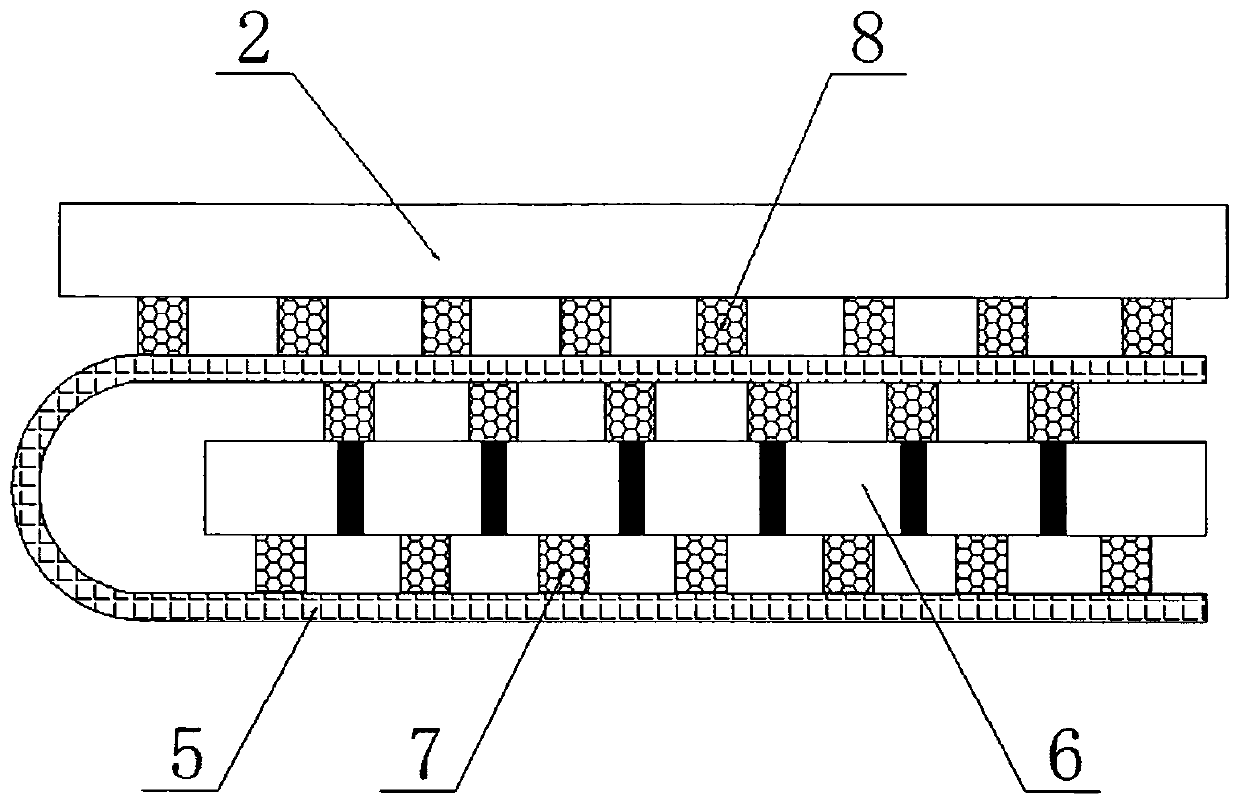
[0045] see image 3 , a packaging structure using a flexible substrate and a TSV chip involved in the present invention, which includes a flexible substrate 5 arranged in a bent manner, a TSV chip 6 is arranged inside the bent part of the flexible substrate 5, and the front and back of the TSV chip 6 Both are connected to the flexible substrate 5 through the first bump 7, and the flip chip 2 is provided on the outer upper surface of the bent flexible substrate 5 through the second bump 8;

Embodiment 2

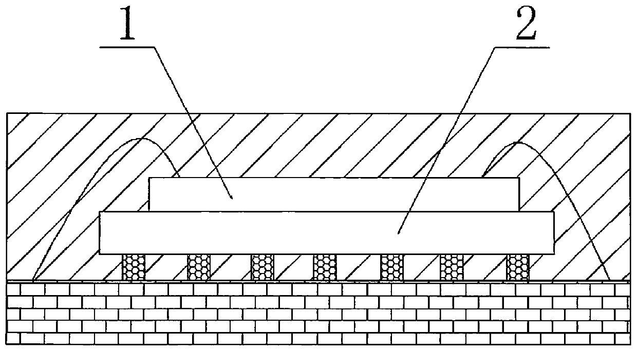
[0047] see Figure 4 , the difference between embodiment 2 and embodiment 1 is that: the upper surface of the outer side of the flexible substrate 5 that is bent and arranged is provided with a soldered chip 1, a flip chip 2 or an SMT component 9;

Embodiment 3

[0049] see Figure 5 The difference between embodiment 3 and embodiment 1 is that: the flexible substrate 5 is bent multiple times, and a TSV chip 6 is arranged inside each bent portion.

[0050] Its process steps are as follows:

[0051] Step 1, see Image 6 , the chip is processed by TSV according to the requirements, so as to lead the circuit on the surface of the chip to the back of the chip;

[0052] Step two, see Figure 7 , The bumps are made on the front and back of the TSV chip. Before making the bumps, the rewiring process can be added according to the actual needs to realize the rewiring on the surface of the TSV chip, so that the layout of the TSV and the bumps is more reasonable;

[0053] Step three, see Figure 8 , mount the TSV chip on the flexible substrate by the flip-chip process;

[0054] Step 4, see Figure 9 , bending the flexible substrate, welding the other side of the TSV chip to the other side of the bent flexible substrate, so as to realize the ...


PUM


Abstract

The invention relates to a packaging structure adopting a flexible substrate and a TSV chip and a manufacturing method of the packaging structure. The packaging structure comprises a flexible substrate (5) which is arranged in a bending manner. A TSV chip (6) is arranged at the inner side of the bending portion of the flexible substrate (5), and the front face and the back face of the TSV chip (6)are connected with the flexible substrate (5) through first protruding blocks (7). A welding chip (1), a flip chip (2) or an SMT component (9) is arranged on the upper surface of the flexible substrate (5) which is arranged in a bending mode. According to the invention, the TSV chip is mounted on the flexible substrate, the flexible substrate is welded on the other surface of the TSV chip after being bent, and a bonding pad for mounting a top chip or a component is arranged on the upward surface of the flexible substrate after the flexible substrate is bent, so that the chip or the componentcan be directly mounted on the flexible substrate.

Description

technical field [0001] The invention relates to a packaging structure adopting a flexible substrate and a TSV (through-silicon via) chip and a manufacturing method thereof, belonging to the technical field of semiconductor packaging. Background technique [0002] There are two main ways of stacking products at present: [0003] The first is a common stacking product, its structure is to stack chips directly on the chip, then wire bonding, and then encapsulation (such as figure 1 shown). This structure has restrictions on the top chip, which can only be a bonded chip; [0004] The second is to use POP technology to stack packages on top of the package (such as figure 2 As shown), since two independent packages are stacked, the size of the final overall package structure will be relatively thick. Contents of the invention [0005] The technical problem to be solved by the present invention is to provide a packaging structure using a flexible substrate and a TSV chip and...

Claims


Application Information

Patent Timeline
Patent Type & Authority Applications(China)
IPC IPC(8): H01L23/538H01L21/768
CPCH01L21/76898H01L23/5384H01L23/5387
Inventor 杨志缪富军赵励强
Owner JCET GROUP CO LTD
Why Eureka
Try Eureka