High-voltage device and low-voltage device integrated structure and integrated method

A technology of high-voltage devices and low-voltage devices, which is applied in the field of semiconductor integrated circuit manufacturing, can solve the problems of large device area and light doping concentration, and achieve the effects of reducing device area, low cost, and reducing width

Active Publication Date: 2017-03-01
SHANGHAI HUAHONG GRACE SEMICON MFG CORP
View PDF6 Cites 0 Cited by
  • Summary
  • Abstract
  • Description
  • Claims
  • Application Information

AI Technical Summary

Problems solved by technology

Because the junction depths of the P-type well region 106 and the N-type well region 102 are equivalent, within the junction depth range of the P-type well region 106, the distance between the depletion lines of two adjacent N-type well regions 102 is relatively small. But at the bottom of the P-type well region 106, the doping of the bottom is the P-type doping of the silicon substrate 101, and the doping concentration is relatively light, so that the depletion at the bottom of the P-type well region 106 The range of the region is relatively large, and the distance between the depletion lines of two adjacent N-type well regions 102 is relatively small.
When the depletion lines of the two adjacent N-type well regions 102 at the bottom of the P-type well region 106 are connected so that the two adjacent N-type well regions 102 are connected to each other, in order to avoid the two The penetration between two adjacent N-type well regions 102 needs to make the width of the field oxygen isolation structure 103a between two adjacent N-type well regions 102 larger, which will make the area of ​​the device too large. Big

Method used


Image

  • High-voltage device and low-voltage device integrated structure and integrated method
  • High-voltage device and low-voltage device integrated structure and integrated method
  • High-voltage device and low-voltage device integrated structure and integrated method

Examples


Embodiment Construction

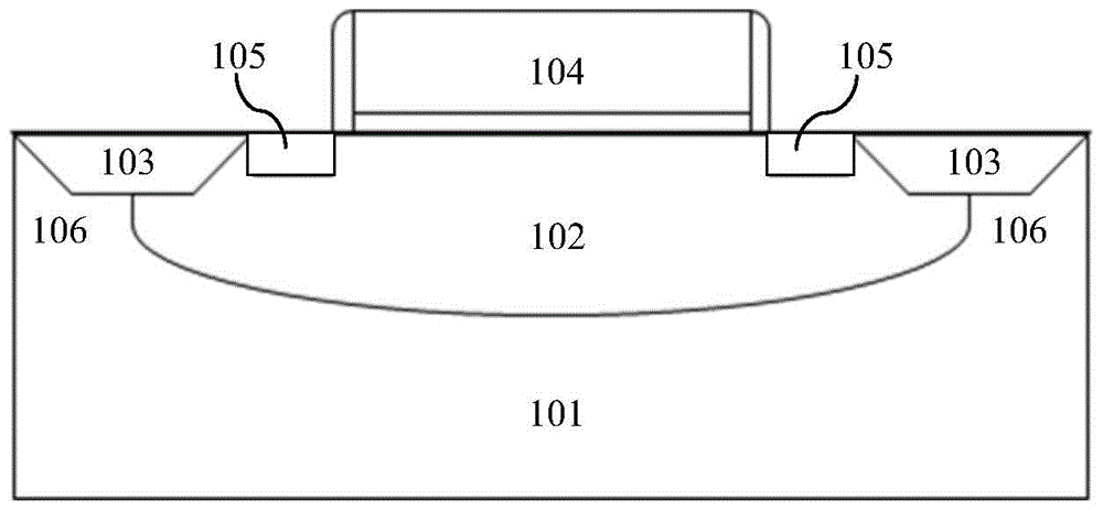
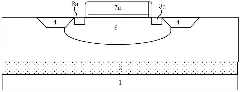
[0038] Such as image 3 As shown, it is a schematic diagram of an NMOS transistor of a low-voltage device with an integrated structure in an embodiment of the present invention; Figure 4 Shown is the schematic diagram of the PMOS tube of the low-voltage device of the integrated structure of the embodiment of the present invention; Figure 5 Shown is a schematic diagram of an N-type high-voltage device with an integrated structure in an embodiment of the present invention; as Figure 6 Shown is a schematic diagram of a P-type high-voltage device with an integrated structure according to an embodiment of the present invention. The low-voltage device of the integrated structure of the high-voltage device and the low-voltage device in the embodiment of the present invention is a CMOS device, and the CMOS device includes an NMOS transistor and a PMOS transistor; the breakdown voltage of the high-voltage device is greater than that of the low-voltage device.

[0039] Both the low...


PUM


Abstract

The invention discloses a high-voltage device and low-voltage device integrating structure. A high-voltage device and a low-voltage device are integrated on a same P-type silicon substrate. A P-type suspended deep well having the same area as the silicon substrate is formed in the silicon substrate. An N-type deep well is formed in part of the area of the silicon substrate. The N-type deep well is disposed on the top of the P-type suspended deep well and contacts the P-type suspended deep well. A channel region, a drain expansion region and an isolated well region of the high-voltage device are composed of the same N-type wells or P-type wells as the low-voltage device. In the region beyond the N-type deep well, the P-type suspended deep well can isolate the N-type wells on the top thereof. The N-type deep well can isolate the P-type wells on the top thereof. The invention further discloses a high-voltage device and low-voltage device integrating method. The high-voltage device and the low-voltage device can be integrated with low cost and without the need for new implantation masks, the parameters of the low-voltage device can be kept unchanged, the width of the isolation region between low-voltage devices can be reduced, the device area can be reduced, and the latch-up effect of the whole circuit can be improved.

Description

technical field [0001] The invention relates to the field of semiconductor integrated circuit manufacturing, in particular to an integrated structure of a high-voltage device and a low-voltage device. The invention also relates to a high-voltage device and a low-voltage device integration method. Background technique [0002] Low-voltage devices are CMOS devices, including NMOS tubes and PMOS tubes; such as figure 1 As shown, it is a structural schematic diagram of an existing low-voltage device; a well region 102 is formed on a P-type silicon substrate 101, and the well region 102 is used as a channel region. For an NMOS transistor, the well region 102 is a P well; PMOS transistor, the well region 102 is an N well. A field oxygen isolation structure 103 is formed on the silicon substrate 101, and an active region is isolated by the field oxygen isolation structure 103. The field oxygen isolation structure 103 is a local field oxygen isolation structure (LOCOS) or a shallo...

Claims


Application Information

Patent Timeline
Patent Type & Authority Patents(China)
IPC IPC(8): H01L27/06H01L29/06H01L21/265H01L21/822
Inventor 郭振强陈瑜邢超
Owner SHANGHAI HUAHONG GRACE SEMICON MFG CORP
Why Eureka
Try Eureka