Semiconductor device and formation method

A semiconductor and device technology, applied in the field of semiconductor devices and formation, can solve problems such as threshold voltage drift and degradation

Active Publication Date: 2015-03-18
SEMICON MFG INT (SHANGHAI) CORP
View PDF4 Cites 8 Cited by
  • Summary
  • Abstract
  • Description
  • Claims
  • Application Information

AI Technical Summary

Problems solved by technology

[0004] However, since there is no shallow trench isolation structure formed between adjacent MOS transistors, there may be leakage current betw

Method used


Image

  • Semiconductor device and formation method
  • Semiconductor device and formation method
  • Semiconductor device and formation method

Examples


Embodiment Construction

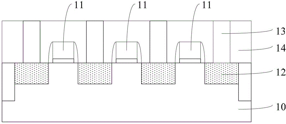
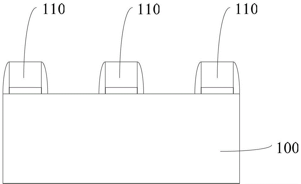
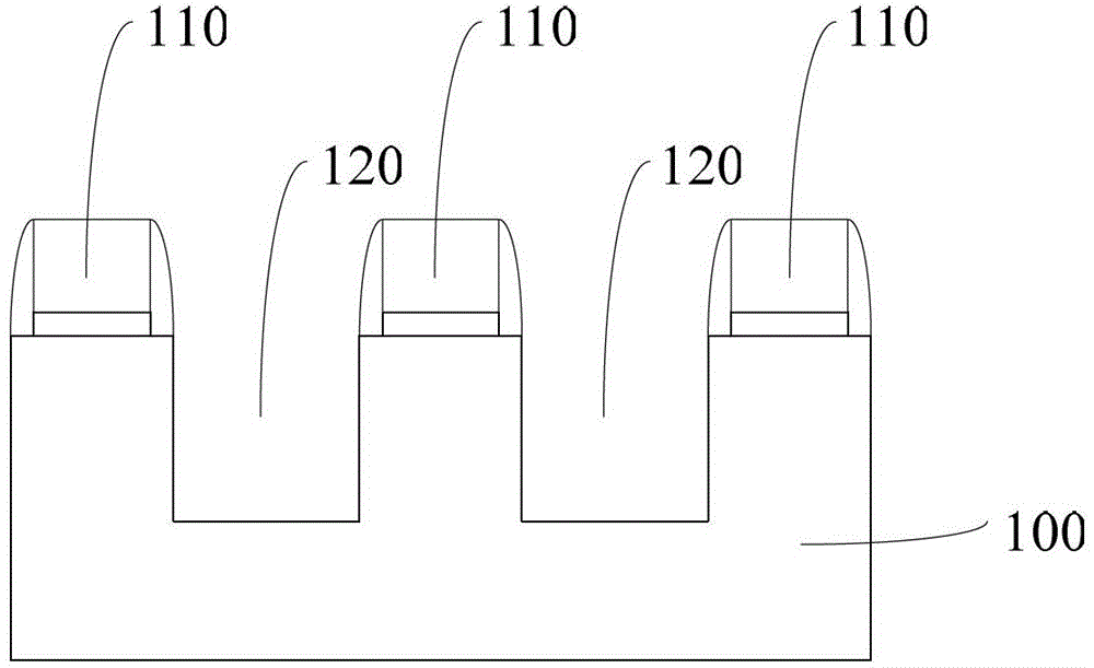
[0026] As described in the background technology, figure 1 In the semiconductor device shown, since the shallow trench isolation structure is not formed between adjacent MOS transistors, there may be leakage current between the channel regions of different MOS transistors, causing problems such as crosstalk, noise margin degradation, and threshold voltage drift. , for this reason, the present invention provides a kind of semiconductor device and its forming method, and the forming method of described semiconductor device comprises: form trench in the semiconductor substrate between adjacent gate structure, utilize selective epitaxial process to form trench in trench An epitaxial layer with protruding morphology is formed on the bottom surface; an insulating layer is formed in the epitaxial layer; a stress layer is formed in the groove, and the stress layer is used as a source and drain region. Since trenches are formed in the semiconductor substrate between adjacent gate struc...


PUM


Abstract

Disclosed are a semiconductor device and a formation method. The formation method of the semiconductor device includes the following steps: forming grooves in a semiconductor substrate between adjacent gate structures and using a selective epitaxy technology to form epitaxy layers with a projection morphology on the surfaces of the bottoms of the grooves; processing the epitaxy layers so that insulating layers are formed; and forming stress layers in the grooves, wherein the stress layers are used as source and drain regions. The insulating layers are capable of reducing the leakage current between channel regions of two adjacent MOS transistors and because the epitaxy layers have a projection morphology, the stress layers corresponding to the middle positions of the grooves are smaller in thickness and the stress layers corresponding to the side-wall positions of the grooves are larger so that reduction of the leakage current between the channel regions of the two adjacent MOS transistors is facilitated and a stress action generated by the stress layers on the channel regions of the MOS transistors is not affected.

Description

technical field [0001] The invention relates to semiconductor manufacturing technology, in particular to a semiconductor device and a forming method. Background technique [0002] In the field of semiconductor manufacturing, with the development of integration and miniaturization of semiconductor devices, in order to further improve chip utilization and increase chip integration, in some semiconductor devices, several MOS transistors are arranged side by side and reduced by sharing source and drain regions. occupied chip area. [0003] Please refer to figure 1 , is a schematic cross-sectional structure diagram of a semiconductor device in which multiple MOS transistors share a source region and a drain region in the prior art, including: a semiconductor substrate 10, a plurality of gate structures 11 arranged in parallel on the surface of the semiconductor substrate 10, located on the The trenches (not shown) in the semiconductor substrate 10 on both sides of the gate stru...

Claims


Application Information

Patent Timeline
IPC IPC(8): H01L27/146H01L21/8238
Inventor 洪中山
Owner SEMICON MFG INT (SHANGHAI) CORP
Why Eureka
Try Eureka