Radio frequency ldmos device and manufacturing method thereof

A manufacturing method and device technology, applied in semiconductor/solid-state device manufacturing, semiconductor devices, electrical components, etc., can solve problems such as radio frequency performance limitations

Active Publication Date: 2018-06-19
SHANGHAI HUAHONG GRACE SEMICON MFG CORP
View PDF4 Cites 0 Cited by
  • Summary
  • Abstract
  • Description
  • Claims
  • Application Information

AI Technical Summary

Problems solved by technology

The output capacitance of RF LDMOS devices has a great limitation on its RF performance

Method used


Image

  • Radio frequency ldmos device and manufacturing method thereof
  • Radio frequency ldmos device and manufacturing method thereof
  • Radio frequency ldmos device and manufacturing method thereof

Examples


no. 1 example

[0027] The first embodiment of the manufacturing method of the radio frequency LDMOS device of the present application includes the following steps:

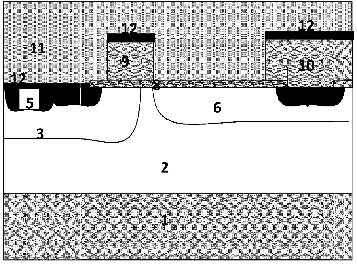
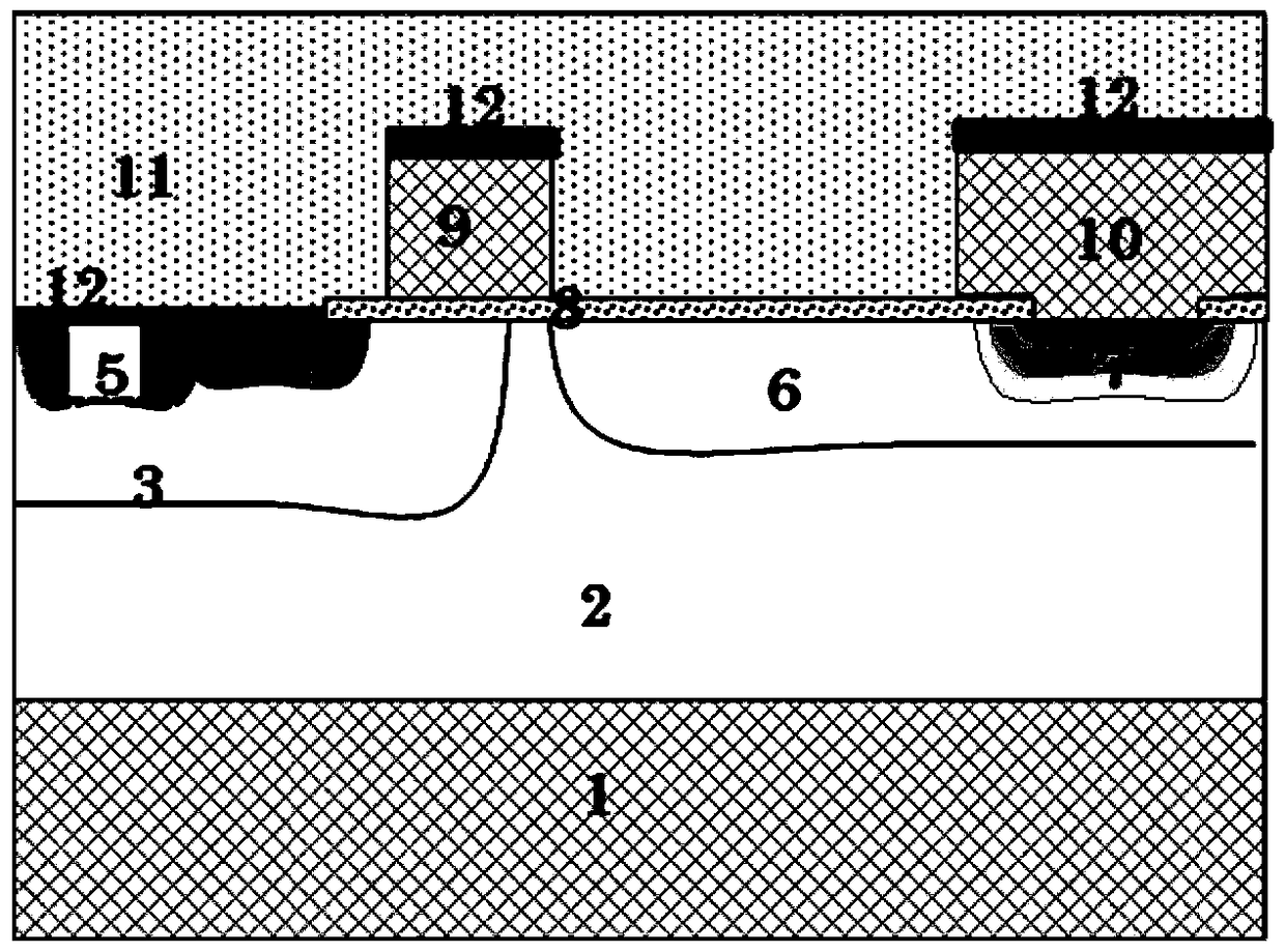
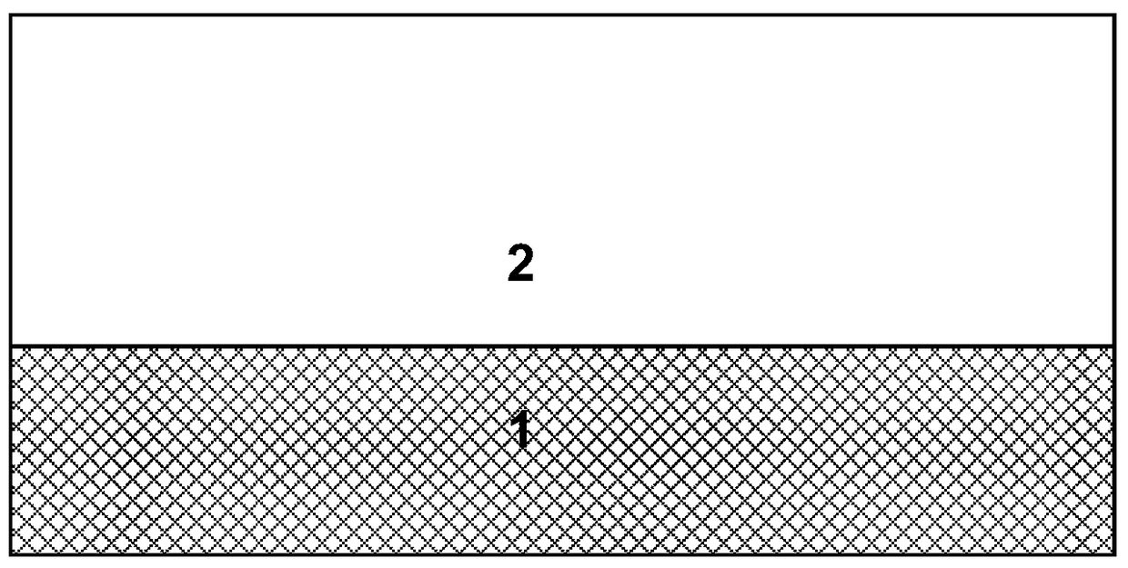
[0028] Step 1, see Figure 3a , epitaxial growth is carried out on the heavily doped p-type substrate 1 to form a layer of lightly doped p-type epitaxial layer 2 . The thickness of the epitaxial layer 2 is, for example, 3 to 15 μm.

[0029] Then, see Figure 3b , forming a ring of isolation structures 2 a on the epitaxial layer 2 . The isolation structure 2 a is silicon oxide, for example, shallow trench isolation (STI) process and local oxidation (LOCOS) process are used. Device isolation is a routine step, which can be omitted without special introduction, and the following figures only show the region between the isolation structures 2a and omit the isolation structure 2a.

[0030] Step 2, see Figure 3c , performing thermal oxidation growth on the epitaxial layer 2 to form a gate oxide layer 8 . The thickness of the ga...


PUM


Abstract

The invention discloses a radio frequency LDMOS device. The radio frequency LDMOS device includes a drain region; a gate oxide layer is arranged above the drain region; the gate oxide layer which is located just above the drain region, is partially removed, so that a window can be formed; a polysilicon plug is arranged on the drain region and the gate oxide layer; a part of the polysilicon plug completely fills the window so as to contact with the drain region; and the other part of the polysilicon plug is located on the gate oxide layer. The radio frequency LDMOS device is characterized in that the doping concentration of the drain region changes gradiently; and in vertical and horizontal directions, the closer the drain region is to a contact portion of the polysilicon plug and the drain region, the higher the doping concentration of the drain region is, and vice versa. The invention also discloses a manufacturing method of the radio frequency LDMOS device. With the radio frequency LDMOS device and the manufacturing method thereof of the invention adopted, the breakdown voltage of the device can be improved, a soft leakage phenomenon can be alleviated, and the output capacitance of the device can be reduced.

Description

technical field [0001] The present application relates to a semiconductor integrated circuit device, in particular to a radio frequency LDMOS (Laterally Diffused MOS Transistor) device. Background technique [0002] see figure 1 , which is an existing RF LDMOS device. There is a lightly doped p-type epitaxial layer 2 on a heavily doped p-type substrate 1 . In the epitaxial layer 2 there is a p-type body region 3 and an n-type drift region 6, the sides of which may or may not be in contact. The body region 3 has a heavily doped n-type source region 4 and a heavily doped p-type body region lead-out region 5, and the sides of the two are in contact. The body region lead-out region 5 is used to lead the body region 3 out. In the drift region 6 there is a heavily doped n-type drain region 7 . There is a gate oxide layer 8 extending from part of the source region 4 to the drain region 7, and its bottom surface contacts the active region 4, the body region 3, and the epitaxial...

Claims


Application Information

Patent Timeline
Patent Type & Authority Patents(China)
IPC IPC(8): H01L29/78H01L29/08H01L21/336
CPCH01L29/0878H01L29/66681H01L29/7816
Inventor 遇寒李昊周正良
Owner SHANGHAI HUAHONG GRACE SEMICON MFG CORP
Why Eureka
Try Eureka