Isolated ldmos device and manufacturing method thereof

An isolated type device technology, which is applied in the manufacture of isolated LDMOS devices and the field of isolated LDMOS devices, can solve the problems of unfavorable industrial production control, increase the peripheral size of devices, and increase process costs, etc., so as to facilitate industrial production control and eliminate The existence of the interface and the effect of reducing the peripheral size of the device

Active Publication Date: 2017-12-05
SHANGHAI HUAHONG GRACE SEMICON MFG CORP
View PDF3 Cites 0 Cited by
  • Summary
  • Abstract
  • Description
  • Claims
  • Application Information

AI Technical Summary

Problems solved by technology

[0011] First, increasing the high-voltage N well 8 will add an additional layer of photolithography, which increases the process cost
[0012] Second, in order to improve the withstand voltage between the isolation well composed of the deep N well 10 and the high voltage N well 8 and the P-type substrate 17 to more than 1.2 times the operating voltage of the device drain, it is necessary to open the area size of the high voltage N well 8 stretched, which increases the peripheral dimensions of the device
[0013] second, figure 1 The position of the junction between the medium-deep N-well 10 and the high-voltage N-well 8 below the polysilicon gate 1 is sensitive to the off-state breakdown voltage of the N-tube, that is, the isolated NLDMOS device. When there is a small fluctuation, the position of the junction of the deep N well 10 and the high voltage N well 8 under the polysilicon gate 1 will also change slightly, and the breakdown voltage of the N transistor will have relatively large fluctuations, which is very important for industrial production control. unfavorable

Method used


Image

  • Isolated ldmos device and manufacturing method thereof
  • Isolated ldmos device and manufacturing method thereof
  • Isolated ldmos device and manufacturing method thereof

Examples


Embodiment Construction

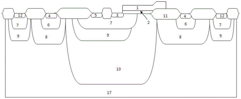
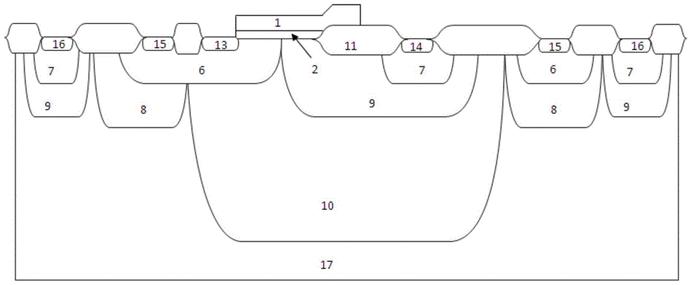
[0046] Such as Figure 4 Shown is the structural diagram of the isolated NLDMOS device of the embodiment of the present invention; as Figure 5 Shown is a structural diagram of an isolated PLDMOS device according to an embodiment of the present invention. The isolated LDMOS device in the embodiment of the present invention includes:

[0047] The deep N well 18 is formed in a P-type substrate such as a silicon substrate 17, and a plurality of field oxide layers 11 are formed on the surface of the P-type substrate 17, and the field oxide layers 11 are used to realize isolation between active regions, The field oxide layer 11 is shallow trench isolation field oxide (STI) or local field oxide (LOCOS).

[0048] The deep N well 18 is divided into an upper part and a lower part, the lower part is composed of a deep N well implanted region, the upper part is composed of a P-type implanted region superimposed on the deep N well implanted region, and the deep N well implanted region i...


PUM


Abstract

The invention discloses an isolated LDMOS device. A deep N-well is divided into an upper part and a lower part and comprises the source region, the drain region and the body region of the device. An isolating ring is formed around the deep N-well. The off-state breakdown voltage of an N pipe and the breakdown voltage of a parasite PN junction between the N-type region of the N pipe or a P pipe and the isolating ring are adjusted by the doping concentration of the upper part. The longitudinal punch-through voltage of a parasite PNP transistor of the N pipe or the P pipe is adjusted by the doping concentration of the lower part. According to the isolated LDMOS device, a process window of device design can be enlarged, integration of the N pipe and the P pipe is facilitated, and application of the N pipe and the P pipe in high-voltage side switches is facilitated; a high-voltage deep N-well is eliminated, and therefore photoetching of a layer is eliminated, the process cost is lowered, and the peripheral area of the device is reduced; the fluctuation influence to the off-state breakdown voltage of the N pipe from the change of the junction position of a high-voltage N-well and the deep N-well can be eliminated, and industrial production control is easy. The invention further discloses a manufacturing method of the isolated LDMOS device.

Description

technical field [0001] The invention relates to the field of manufacturing semiconductor integrated circuits, in particular to an isolation type LDMOS device; the invention also relates to a manufacturing method of the isolation type LDMOS device. Background technique [0002] In the prior art, isolated LDMOS devices are divided into N-type devices, that is, isolated NLDMOS devices, and P-type devices, that is, isolated LDPMOS devices; sometimes, isolated NLDMOS devices and isolated PLDMOS devices are integrated on the same substrate for preparation. [0003] Such as figure 1 Shown is a structural diagram of an existing isolated NLDMOS device; a deep N well 10 is formed in a P-type substrate 17 . A body region composed of a high-voltage P well 9 and a low-voltage P well 7 is formed in the deep N well 10, and a body region lead-out region 5 and a source region 3 are formed in the body region; The field oxide layer 11 is used to realize isolation between active regions, and ...

Claims


Application Information

Patent Timeline
Patent Type & Authority Patents(China)
IPC IPC(8): H01L29/78H01L29/06H01L21/336H01L21/265
CPCH01L21/265H01L29/06H01L29/0611H01L29/66681H01L29/7816
Inventor 李喆罗啸
Owner SHANGHAI HUAHONG GRACE SEMICON MFG CORP
Why Eureka
Try Eureka