goa circuit for liquid crystal display device

A liquid crystal display device and circuit technology, applied in the field of GOA circuits, can solve the problems of complex CMOS circuit structure and difficulty in designing ultra-narrow borders, and achieve the effect of ensuring stability

Active Publication Date: 2017-01-18
TCL CHINA STAR OPTOELECTRONICS TECH CO LTD
View PDF7 Cites 0 Cited by
  • Summary
  • Abstract
  • Description
  • Claims
  • Application Information

AI Technical Summary

Problems solved by technology

[0005] With the development of low-temperature polysilicon semiconductor (LTPS) thin-film transistor (TFT), and due to the ultra-high carrier mobility characteristics of LTPS semiconductor itself, the corresponding panel peripheral integrated circuit, that is, GOA, has become the focus of attention, and many People have invested in the related technology research of system integration panel (System on Panel, SOP), and it has gradually become a reality. Since LTPS can use ion arrangement technology to adjust the TFT type, NMOS, PMOS and CMOS circuits can be selected, but CMOS and NMOS are in the optical Compared with PMOS, the cost of the cover will be greatly increased, and the circuit structure of CMOS is too complicated, so it is difficult to achieve the design of ultra-narrow bezel. This is particularly important when targeting small-sized display devices. PMOS circuits are cost and circuit structures The advantages on the market make it gradually become the mainstream

Method used


Image

  • goa circuit for liquid crystal display device
  • goa circuit for liquid crystal display device
  • goa circuit for liquid crystal display device

Examples


Embodiment Construction

[0059] The following descriptions of the various embodiments refer to the accompanying drawings to illustrate specific embodiments in which the present invention can be practiced. The directional terms mentioned in the present invention, such as "up", "down", "front", "back", "left", "right", "inside", "outside", "side", etc., are for reference only The orientation of the attached schema. Therefore, the directional terms used are used to illustrate and understand the present invention, but not to limit the present invention.

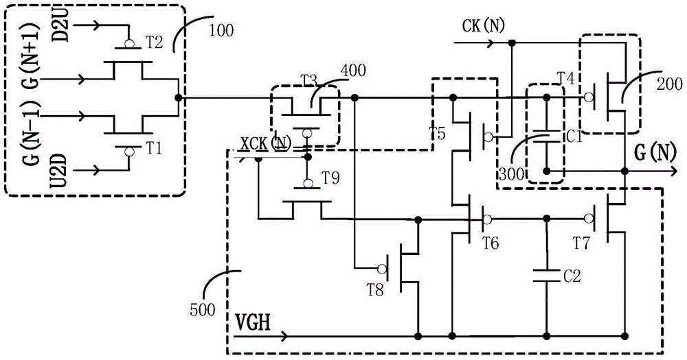
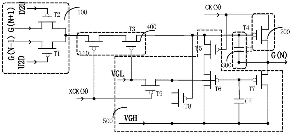
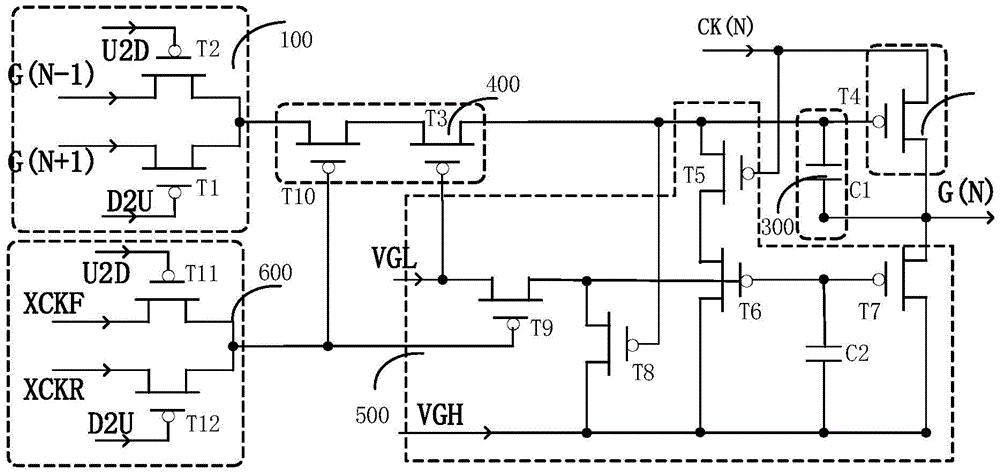
[0060] figure 1 It is a schematic circuit diagram of the GOA of the first preferred embodiment of the present invention. The GOA circuit is used in a liquid crystal display device, and the liquid crystal display device includes a plurality of scanning lines, and the GOA circuit includes a plurality of cascaded shift register units. The Nth-level shift register unit controls charging of the Nth-level scan lines. The Nth stage shift register unit inclu...


PUM


Abstract

The invention discloses a gate driver on array (Gate Driver On Array; GOA) circuit for a liquid crystal display device. The liquid crystal display device includes a plurality of scanning lines, and the GOA circuit includes a plurality of cascaded shift buffers. unit. The Nth-level shift register unit controls charging of the Nth-level scan lines. The Nth stage shift register unit includes a forward and reverse scanning control circuit, a pull-up circuit, a bootstrap capacitor circuit, a gate signal point leakage prevention circuit and a pull-down maintenance circuit. The bootstrap capacitor circuit, the gate signal point leakage prevention circuit and the pull-down maintaining circuit are jointly connected to form a gate signal point for improving the stability of the gate signal point and reducing the use of switches.

Description

[0001] 【Technical field】 [0002] The present invention relates to the field of liquid crystal display technology, in particular to a GOA (GateDriver On Array, array substrate row scanning drive) based on LTPS (Low-TemperaturePoly-Si) PMOS (P-channel Metal Oxide Semiconductor) for liquid crystal display devices circuit. [0003] 【Background technique】 [0004] GOA is a technology that uses the existing thin-film transistor liquid crystal display array (Array) process to fabricate the gate (Gate) line scanning drive signal circuit on the array substrate to realize the drive mode of progressive scanning of the gate. [0005] With the development of low-temperature polysilicon semiconductor (LTPS) thin-film transistor (TFT), and due to the ultra-high carrier mobility characteristics of LTPS semiconductor itself, the corresponding panel peripheral integrated circuit, that is, GOA, has become the focus of attention, and many People have invested in the related technology research o...

Claims


Application Information

Patent Timeline
Patent Type & Authority Patents(China)
IPC IPC(8): G09G3/36
CPCG09G3/3677G09G2300/0408G09G2310/0286G11C19/28G09G2310/08G09G2230/00G09G2330/04
Inventor 肖军城
Owner TCL CHINA STAR OPTOELECTRONICS TECH CO LTD
Why Eureka
Try Eureka