
GOA circuit for liquid crystal display device

A liquid crystal display device and circuit technology, applied in the field of GOA circuits, can solve the problems of difficult to achieve ultra-narrow frame design, complex CMOS circuit structure, etc., and achieve the effects of reducing the number of transistors, improving stability, and increasing driving capability.

Active Publication Date: 2015-04-22
TCL CHINA STAR OPTOELECTRONICS TECH CO LTD
View PDF5 Cites 50 Cited by
  • Summary
  • Abstract
  • Description
  • Claims
  • Application Information

AI Technical Summary

Problems solved by technology

[0003] With the development of low-temperature polysilicon semiconductor (LTPS) thin-film transistor (TFT), and due to the ultra-high carrier mobility characteristics of LTPS semiconductor itself, the corresponding panel peripheral integrated circuit, that is, GOA, has become the focus of attention, and many People have invested in the related technology research of system integration panel (System on Panel, SOP), and it has gradually become a reality. Since LTPS can use ion arrangement technology to adjust the TFT type, NMOS, PMOS and CMOS circuits can be selected, but CMOS and NMOS are in the optical Compared with PMOS, the cost of the cover will be greatly increased, and the circuit structure of CMOS is too complicated, so it is difficult to achieve the design of ultra-narrow bezel. This is particularly important when targeting small-sized display devices. PMOS circuits are cost and circuit structures The advantages on the market make it gradually become the mainstream

Method used


Image

  • GOA circuit for liquid crystal display device
  • GOA circuit for liquid crystal display device

Examples


Embodiment Construction

[0034] The following descriptions of the various embodiments refer to the accompanying drawings to illustrate specific embodiments in which the present invention can be practiced. The directional terms mentioned in the present invention, such as "up", "down", "front", "back", "left", "right", "inside", "outside", "side", etc., are for reference only The orientation of the attached schema. Therefore, the directional terms used are used to illustrate and understand the present invention, but not to limit the present invention.

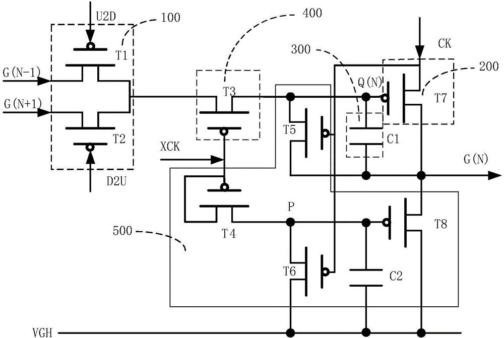
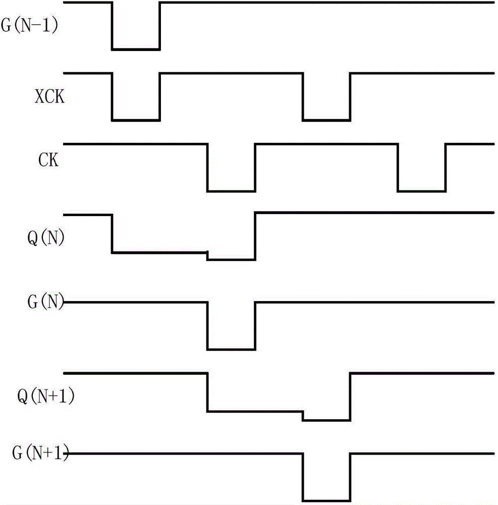
[0035] figure 1 It is a schematic circuit diagram of the GOA in the present invention. The liquid crystal display device includes a plurality of scan lines, and the GOA circuit includes a plurality of cascaded GOA units. The Nth-level GOA unit controls charging of the Nth-level scan lines in the display area. The Nth level GOA unit includes a forward and reverse scanning control circuit (100), a pull-up circuit (200), a bootstrap capacitor circuit (3...


PUM


Abstract

The invention discloses a gate driver on array (GOA) circuit for a liquid crystal display device. The liquid crystal display device comprises multiple scanning lines, and the GOA circuit comprises multiple cascaded GOA units. The Nth scanning line of the display area is charged by a Nth level GOA unit control, and the Nth level GOA unit comprises a forward and reverse scanning control circuit, a pull-up circuit, a bootstrap capacitor circuit, a pull-up control circuit and a drop-down holding circuit. The pull-up circuit, the bootstrap capacitor circuit, the pull-up control circuit and the drop-down holding circuit are connected with a grid signal point. The pull-up circuit, the bootstrap capacitor circuit and the drop-down holding circuit are connected with the Nth scanning line. The forward and reverse scanning control circuit is connected with a (N-1)th scanning line and the (N+1)th scanning line. The GOA circuit for the liquid crystal display device is used for improving the stability of the grid signal point and reducing the usage of transistors.

Description

【Technical field】 [0001] The present invention relates to the field of liquid crystal display technology, in particular to a GOA (Gate Driver On Array, array substrate line scanning) based on LTPS (Low-Temperature Poly-Si) PMOS (P-channel Metal Oxide Semiconductor) used for liquid crystal display devices Drive circuit. 【Background technique】 [0002] GOA is a technology that uses the existing thin-film transistor liquid crystal display array (Array) process to fabricate the gate (Gate) line scanning drive signal circuit on the array substrate to realize the drive mode of progressive scanning of the gate. [0003] With the development of low-temperature polysilicon semiconductor (LTPS) thin-film transistor (TFT), and due to the ultra-high carrier mobility characteristics of LTPS semiconductor itself, the corresponding panel peripheral integrated circuit, that is, GOA, has become the focus of attention, and many People have invested in the related technology research of syste...

Claims


Application Information

Patent Timeline
Patent Type & Authority Applications(China)
IPC IPC(8): G09G3/36
CPCG02F1/13454G09G3/3677G09G2300/0408G09G2310/0283G09G2310/0286G09G2310/08G11C19/28G02F1/13G02F1/133G09G2230/00
Inventor 肖军城赵莽田勇
Owner TCL CHINA STAR OPTOELECTRONICS TECH CO LTD
Learn More