A kind of flexible mold for making flexible circuit board and preparation method thereof

A technology for flexible circuit boards and flexible molds, which is used in the removal of conductive materials by chemical/electrolytic methods, printed circuit manufacturing, printed circuits, etc. and other problems to achieve the effect of reducing production costs, improving quality, and reducing graphics deformation

Active Publication Date: 2018-01-16
SHANGHAI LIANGZI HUIJING ELECTRONICS CO LTD
View PDF5 Cites 0 Cited by
  • Summary
  • Abstract
  • Description
  • Claims
  • Application Information

AI Technical Summary

Problems solved by technology

[0008] In view of the above-mentioned shortcomings of the prior art, the purpose of the present invention is to provide a flexible mold for the production of flexible circuit boards and its preparation method, which is used to solve the complex and high cost of the preparation process of the flexible mold in the prior art, which makes The problem of the corresponding increase in the production cost of flexible circuit boards

Method used


Image

  • A kind of flexible mold for making flexible circuit board and preparation method thereof
  • A kind of flexible mold for making flexible circuit board and preparation method thereof
  • A kind of flexible mold for making flexible circuit board and preparation method thereof

Examples


Embodiment 1

[0048] The invention provides a method for preparing a flexible mold for making a flexible circuit board, which at least includes the following steps:

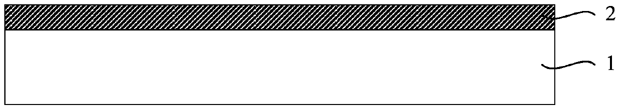
[0049] See first figure 1 , providing a flexible substrate 1 whose surface is covered with a metal layer 2 .

[0050]Specifically, the flexible substrate 1 includes but not limited to PI substrate, PTFE substrate or PET substrate. Among them, PI (Polyimid, polyimide) substrate is widely used in the field of flexible circuit boards, and is a traditional soft board material; PTFE (polytetrafluoroethylene, polytetrafluoroethylene film) has excellent performance in chemical corrosion resistance, and has excellent Flexibility; PET (Polyethylene terephthalate, polyethylene terephthalate) substrate is a highly transparent insulating material and is a common flexible substrate.

[0051] The material of the metal layer 2 includes but not limited to one or more of Au, Ag, Cu, Al, that is, the metal layer 2 can be a single metal or an ...

Embodiment 2

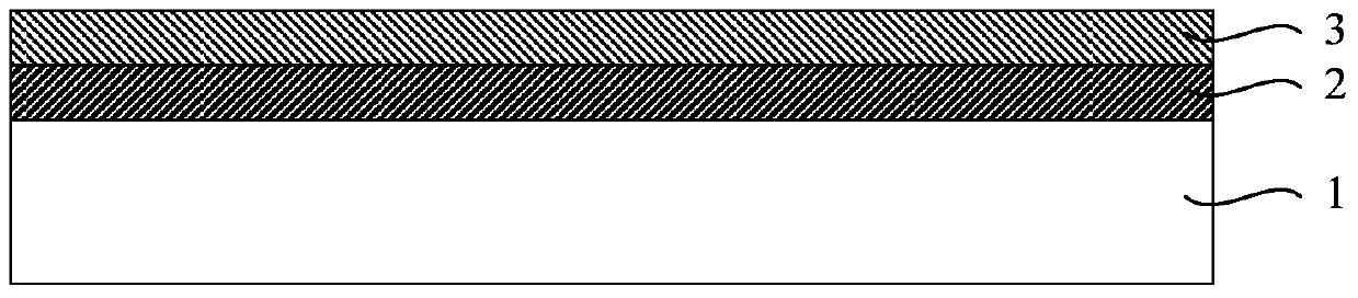
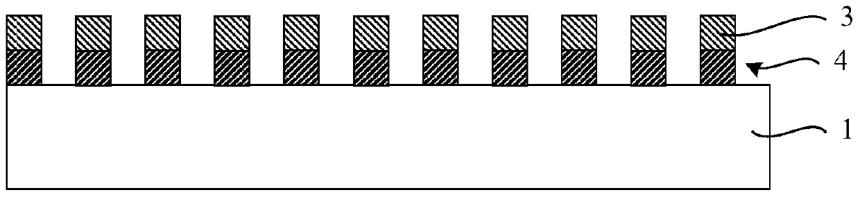
[0062] The present invention also provides a flexible mold for making flexible circuit boards, please refer to Figure 4 , the flexible mold includes a flexible substrate 1 and a metal circuit pattern 4 sequentially from bottom to top.

[0063] Specifically, the flexible substrate includes but not limited to PI substrate, PTFE substrate or PET substrate, and the material of the metal circuit pattern includes but not limited to one or more of Au, Ag, Cu, Al.

[0064] In this embodiment, the flexible substrate 1 is preferably a PI substrate, and the material of the metal circuit pattern 4 is preferably Cu. The line width range of the metal circuit pattern 4 is 20-800 μm, which can meet the requirement of making highly integrated flexible circuit boards.

[0065] In another embodiment, the bottom of the gap of the metal circuit pattern 4 does not reach the flexible substrate 1, such as Figure 5 shown. Since the bottom of the metal circuit is still connected by metal, it can e...

Embodiment 3

[0069] The method that adopts flexible mold of the present invention to make flexible circuit board is as follows:

[0070] See first Image 6 , providing a flexible substrate. It should be pointed out that at least one of the flexible substrate 1 used in the flexible mold and the flexible substrate must have high transparency, so as to facilitate the penetration of ultraviolet light in the subsequent ultraviolet curing process. In this embodiment, it is preferable to use a flexible mold in which the flexible substrate 1 is a PI substrate and the metal circuit pattern 4 is Cu. Since the transparency of the PI substrate is not high, the flexible substrate takes the highly transparent PET film 5 as an example.

[0071] see next Figure 7 , coating a layer of UV glue 6 on the surface of the PET film 5 .

[0072] then see Figure 8 , align and contact the flexible mold with the PET film 5 coated with UV glue 6 on the surface, and then form the UV glue in the embossed area thr...


PUM


Abstract

The invention provides a flexible die and a production method for manufacturing flexible printed circuit boards. The production method includes the steps of providing a flexible substrate having a metal layer covering the surface thereof; attaching a dry film to the surface of the metal layer, patterning the dry film, and using the patterned dry film as a mask to perform etching on the metal layer so as to obtain a metal circuit pattern; removing the dry film to obtain the flexible substrate and a flexible die of the metal circuit pattern from top to bottom. The production method has the advantages that the process is simple, die cost is low, and the requirement of the flexible printed circuit board industry for conductivity of the flexible printed circuit boards can be met when the production method is applied to the production of the flexible printed circuit boards. The flexible die is composed of the flexible substrate and the metal circuit pattern; the flexible substrate meets the requirement for uniformity of nanoimprinting on a large-area substrate; the metal circuit pattern is of high hardness, pattern deformation can be decreased during imprinting, and quality of the flexible printed circuit boards produced by nanoimprinting is improved.

Description

technical field [0001] The invention belongs to the field of flexible circuit boards, and relates to a flexible mold for making flexible circuit boards and a preparation method thereof. Background technique [0002] In recent years, ever-changing electronic products continue to develop in the direction of small size, light weight, and complex functions. Printed circuit board (PCB), as an indispensable main part of electronic products, provides the interconnection of electrical signals and the support of electronic components. Especially the flexible printed circuit board (Flexible Printed Circuit, FPC), is one of the industries with the most vigorous development momentum. [0003] Traditional soft board materials are mainly based on the three-layer structure of polyimide (PI) film / adhesive / copper foil, and the adhesive is mainly Epoxy / Acrylic, but the heat resistance and dimensional stability of the adhesive are not good. Best, the long-term use temperature is limited to 1...

Claims


Application Information

Patent Timeline
Patent Type & Authority Patents(China)
IPC IPC(8): H05K3/00H05K3/06
Inventor 杨恺林晓辉平财明徐厚嘉陈春明
Owner SHANGHAI LIANGZI HUIJING ELECTRONICS CO LTD
Why Eureka
Try Eureka