Chip debugging method and debugging circuit under normal operating mode

A technology of normal working mode and debugging method, which is applied in the direction of measuring electricity, measuring electrical variables, measuring devices, etc., and can solve the problems of complex test sequence output test sequence rapid analysis, etc.

Active Publication Date: 2015-04-22
SHANDONG SINOCHIP SEMICON
View PDF4 Cites 9 Cited by
  • Summary
  • Abstract
  • Description
  • Claims
  • Application Information

AI Technical Summary

Problems solved by technology

[0005] The above is a simple description of the work of ordinary scanning circuits, and its complexity lies in the generation algorithm of the test sequence and the rapid analysis of the output test sequence

Method used


Image

  • Chip debugging method and debugging circuit under normal operating mode
  • Chip debugging method and debugging circuit under normal operating mode
  • Chip debugging method and debugging circuit under normal operating mode

Examples


Embodiment Construction

[0021] The present invention will be further described below in conjunction with the accompanying drawings.

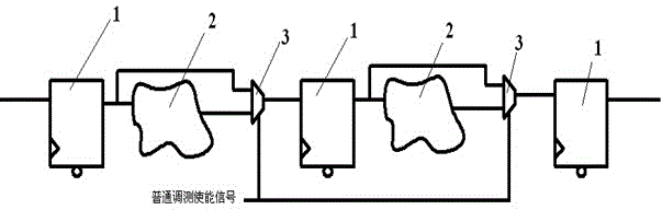
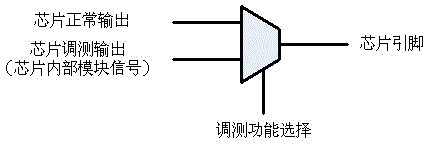
[0022] Usually a chip includes a lot of pins, but these pins will not be used in every working state of the chip at the same time, and the new function definition of the pins that can not be used in the current working state will not affect the normal operation of the chip. Therefore if figure 1 As shown, the chip debugging method in normal working mode provided by the present invention is to use the pin multiplexing technology when the chip pin function is defined, and output the normal function output signal of the chip and the internal signal that needs to be drawn out after multiplexing. To the chip pin, that is, the current output signal of the pin is controlled by the multiplexer, so that the multiplexer can be controlled to output the internal signal as the output value to the pin in the normal working debugging mode.

[0023] Then in the back-end design of the...


PUM


Abstract

The invention discloses a chip debugging method under a normal operating mode. The method comprises the following steps: adopting a pin multiplexing technology when a chip pin function is defined, multiplexing a chip normal function output signal and an internal signal to be led out, outputting the signals to a chip pin, and controlling the current output signal of the pin by virtue of a multiplexer, so that the multiplexer can be controlled to output the internal signal serving as an output value to the pin in a normal operation debugging mode. The invention also discloses a chip debugging circuit under the normal operating mode. According to the method and circuit disclosed by the invention, the debugging function of the chip can be started under the normal operating mode, the signal state of a pre-tested combined logical circuit (port or interior) can be acquired during normal operation of the chip, the fault is positioned, and the problem is confirmed.

Description

technical field [0001] The invention relates to the field of integrated circuit testing, in particular to a chip debugging method and a debugging circuit in a normal working mode. Background technique [0002] When debugging existing chips, the access to the chip debugging port needs to start the debugging function in advance, set the chip to the debugging mode, and then carry out data communication, but in this state the chip cannot achieve the expected design function, so this method can only locate the device Level problems, powerless to deal with logic problems. [0003] After the chip is produced, it is necessary to test whether the function of the chip circuit is consistent with the design. The method is to connect the registers in the circuit in series to form several scan register chains, and input the test sequence at the input end of each scan chain ( That is, "0" and "1" sequence), and then according to the working principle of the register, you can get this sequ...

Claims


Application Information

Patent Timeline
Patent Type & Authority Applications(China)
IPC IPC(8): G01R31/3183
Inventor 刘大铕孙晓宁张洪柳赵阳王运哲刘奇浩
Owner SHANDONG SINOCHIP SEMICON
Why Eureka
Try Eureka