System on chip and control method

A technology of system-on-chip and control method, which is applied in the direction of instrumentation, electrical digital data processing, etc., can solve problems such as technical difficulty and high cost, failure to meet design requirements, and inability to further reduce development and upgrade costs, etc., to achieve rich system products Effect

Inactive Publication Date: 2018-11-30
杭州士兰控股有限公司
View PDF5 Cites 0 Cited by
  • Summary
  • Abstract
  • Description
  • Claims
  • Application Information

AI Technical Summary

Problems solved by technology

[0007] However, using SERDES connection between SOC-A and SOC-B is relatively high in technical difficulty and cost
In addition, dividing the SOC into the digital part SOC-A and the analog part SOC-B cannot meet the user-oriented design requirements, so there are certain limitations and cannot further reduce development and upgrade costs

Method used


Image

  • System on chip and control method
  • System on chip and control method
  • System on chip and control method

Examples


Embodiment Construction

[0041] Various embodiments of the invention will be described in more detail below with reference to the accompanying drawings. In the various drawings, the same elements are denoted by the same or similar reference numerals. For the sake of clarity, various parts in the drawings have not been drawn to scale.

[0042] The invention can be embodied in various forms, some examples of which are described below.

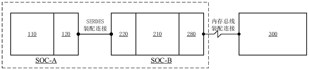
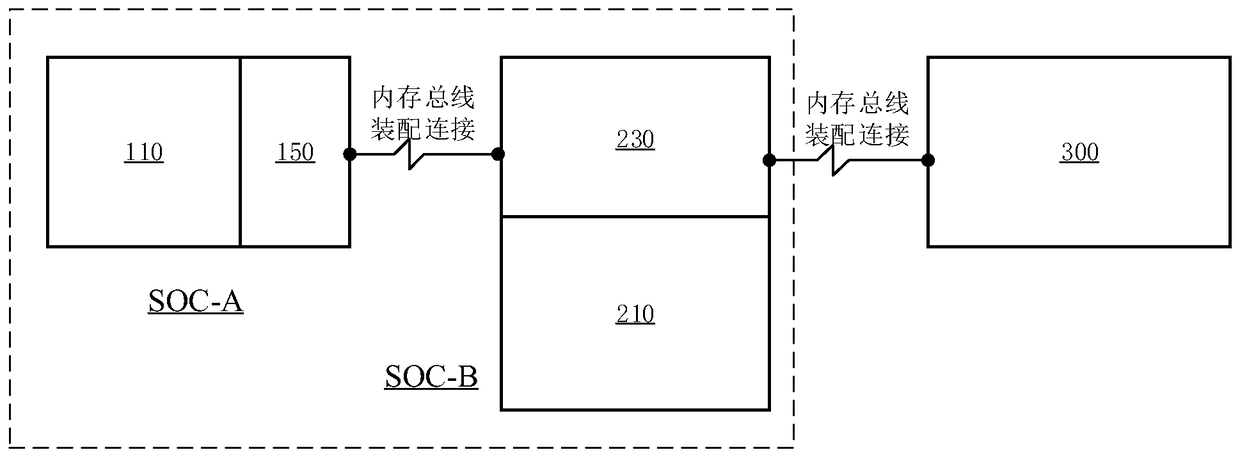
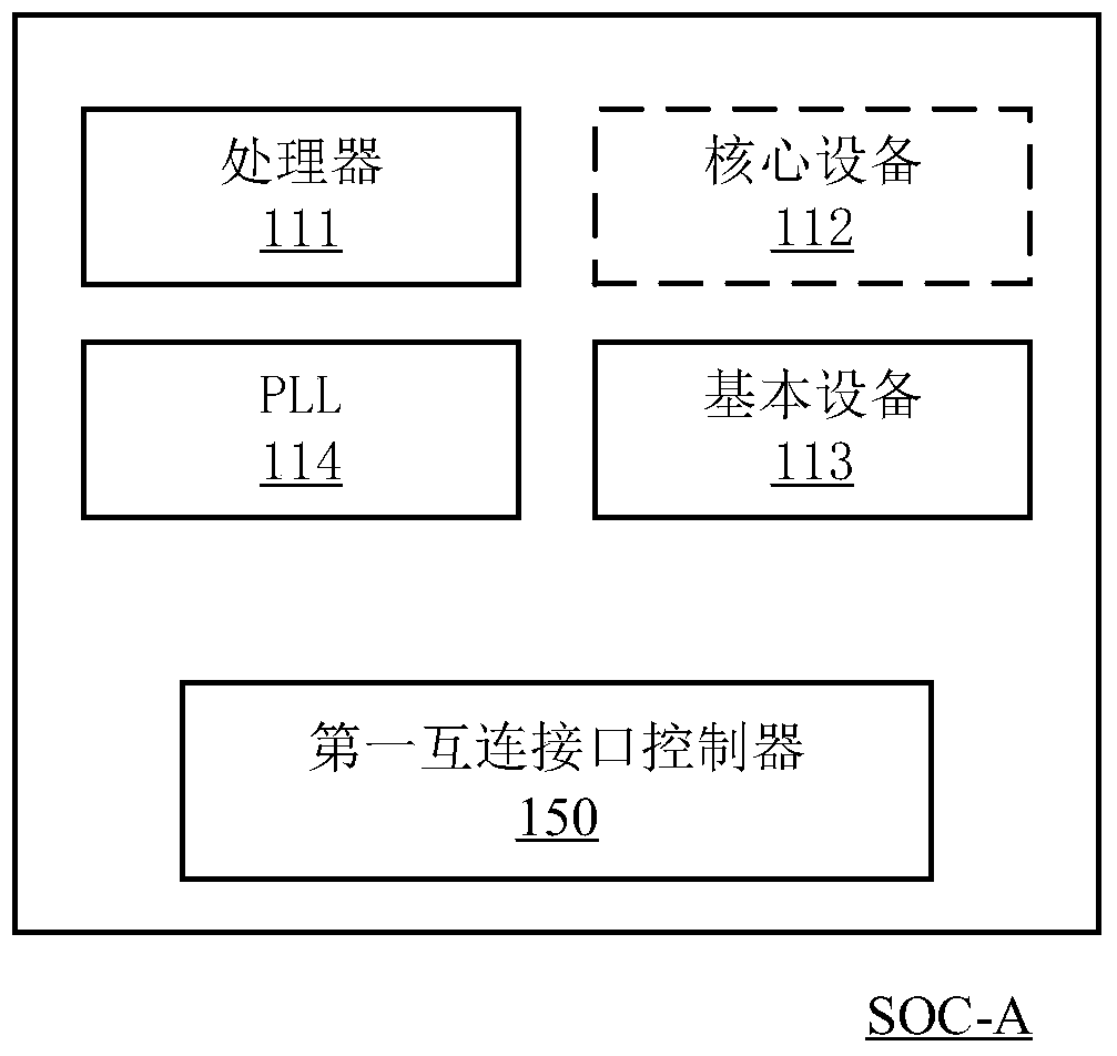
[0043] figure 2 A schematic block diagram of a system on chip and its external memory according to the present invention is shown. As shown in the figure, the SOC is divided into two circuit parts, SOC-A and SOC-B. SOC-A includes a first main function module 110 and a first interconnection interface controller 150 , and SOC-B includes a second main function module 210 and a second interconnection interface controller 230 .

[0044] However, unlike the prior art, a memory bus connection is used between SOC-A and SOC-B. Correspondingly, the first interconnection inte...


PUM


Abstract

The invention discloses a system on chip and a control method. The system on chip comprises a first circuit part and a second circuit part, wherein the first circuit part comprises a first main function module and a first interconnecting interface controller, the second circuit part comprises a second main function module and a second interconnecting interface controller, and the first interconnecting interface controller and the second interconnecting interface controller respectively provide memory interfaces used for interconnecting, so that the first circuit part and the second circuit part are connected through a first memory bus. The system on chip provided by the invention has the advantages that the memory interfaces are adopted for realizing the interconnection between different circuit parts, so that the development cost can be reduced, and the design freedom is provided.

Description

technical field [0001] The invention belongs to chip design technology, and in particular relates to an on-chip system and a control method. Background technique [0002] In the existing system-on-chip (SOC, System on Chip) design method, various digital logic design resources (IP, Intellectual Property) and various analog unit IPs are usually integrated on a single chip to maximize integration. Spend. [0003] Digital logic IP can include central processing unit (CPU), digital signal processor (DSP), counter (TIMER), watchdog (WATCHDOG) and other transaction processing units, graphics, video, audio, encryption and decryption and other computing Unit, various digital interfaces such as SDMMC, Universal Asynchronous Receiver Transmitter (UART), Serial Peripheral Interface (SPI), and protocol layers of various high-speed serial interfaces such as Universal Serial Bus (USB), PCIe, SATA, HDMI, etc. and an on-chip bus connecting various devices, but not limited thereto. Analog...

Claims


Application Information

Patent Timeline
Patent Type & Authority Patents(China)
IPC IPC(8): G06F13/16
CPCG06F13/1642G06F13/28G06F2213/0038
Inventor 张华孙熙文王相如许庆春
Owner 杭州士兰控股有限公司
Why Eureka
Try Eureka