
A Method for Preparing Quadratic Micro-curved Surface Structure by Bitmap Superposition

A curved surface structure and bitmap technology, applied in the manufacture of microstructure devices, microstructure technology, microstructure devices, etc., to achieve high design matching, good flexibility, smooth and delicate etching surface

Active Publication Date: 2017-06-16
INST OF PHYSICS - CHINESE ACAD OF SCI
View PDF3 Cites 0 Cited by
  • Summary
  • Abstract
  • Description
  • Claims
  • Application Information

AI Technical Summary

Problems solved by technology

[0004] The processing of a single micro-curved surface with a certain position and an ideal shape has not been reported

Method used


Image

  • A Method for Preparing Quadratic Micro-curved Surface Structure by Bitmap Superposition
  • A Method for Preparing Quadratic Micro-curved Surface Structure by Bitmap Superposition
  • A Method for Preparing Quadratic Micro-curved Surface Structure by Bitmap Superposition

Examples


Embodiment Construction

[0023] In order to make the object, technical solution and advantages of the present invention clearer, the present invention will be described in further detail below in conjunction with specific embodiments and with reference to the accompanying drawings.

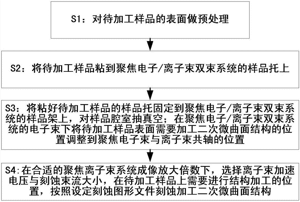
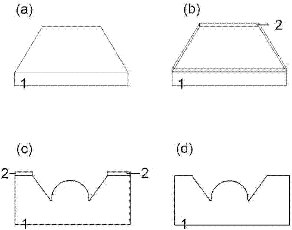
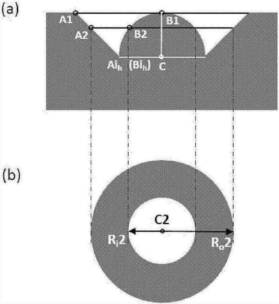
[0024] An embodiment of the present invention provides a method for preparing a combined structure of hemispheres and inclined sidewalls on the surface of a diamond block by means of bitmap superposition. The experiment is performed on a focused electron / ion beam dual-beam Helios NanoLab600i produced by FEI Corporation in the United States. in the system. The steps include: pretreating the surface of the sample to be processed; fixing the sample; injecting the sample and adjusting the coaxiality; selecting a suitable ion acceleration voltage and beam current for etching processing.

[0025] Bitmap file (Bitmap), the extension can be .bmp or .dib. A bitmap is a Windows standard format graphics file, which defines an image...


PUM

PropertyMeasurementUnit
thicknessaaaaaaaaaa
radiusaaaaaaaaaa

Abstract

The invention provides a method for preparing a secondary micro curved surface structure by overlapping bitmaps. The method comprises the steps of S1, preprocessing the surface of a sample to be processed; S2, adhering the sample to be processed on a sample support of a focused election / ion beam double-beam system; S3, fixing the sample support adhered with the sample to be processed on a sample rack of the focused election / ion beam double-beam system, pumping vacuum for a sample cavity, and adjusting the position of the secondary curved surface structure to be processed, of the surface of the sample to be processed to the position in which a focused election beam and an ion beam are coaxial under the electron beam of the focused election / ion beam double-beam system; S4, selecting electron beam acceleration voltage and etching beam stream under proper imaging amplification factors the focused ion beam system, and etching and processing the secondary micro curved surface structure at the secondary micro curved surface structure processing position on the sample to be sampled according to a set etching graph file.

Description

technical field [0001] The invention relates to the technical field of micro-nano device processing, and relates to a method for preparing a quadratic micro-curved surface structure in a bitmap superposition manner in a focused electron / ion beam dual-beam system. Background technique [0002] Due to the needs of optical information technology for miniaturized, arrayed, and integrated optical devices, surface structures such as curved microlenses and their arrays have attracted extensive attention from researchers. For the preparation of microlenses and their arrays, planar processes such as photosensitive glass method, holographic method, photoresist melting method and laser etching method have been developed. These processes can realize the mass production of structural devices, and at the same time meet the current application requirements to a certain extent. However, their disadvantage is that the control of the structural morphology does not fully match the functional ...

Claims


Application Information

Patent Timeline
Patent Type & Authority Patents(China)
IPC IPC(8): H01L21/00H01L21/02H01L21/027B81C1/00
CPCB81C1/00206
Inventor 顾长志姜倩晴唐成春李无瑕金爱子李俊杰
Owner INST OF PHYSICS - CHINESE ACAD OF SCI
Learn More