Printed circuit board and manufacturing method of printed circuit board

A technology of printed circuit board and manufacturing method, which is applied in the direction of multi-layer circuit manufacturing, printed circuit components, and the formation of electrical connection of printed components, can solve the problem of affecting the electrical performance of the printed circuit board, the difficulty of blind holes in the window opening area, and the precise alignment of blind holes. The flow glue is easy to flow into the blind hole and other problems, so as to achieve the effect of not easy to flow, good stability and high removal accuracy

Active Publication Date: 2015-05-20
HUAWEI TECH CO LTD
View PDF5 Cites 7 Cited by
  • Summary
  • Abstract
  • Description
  • Claims
  • Application Information

AI Technical Summary

Problems solved by technology

The disadvantage of this technology is that the window opening area of ​​the prepreg is not easy to be accurately aligned with the blind hole, and the prepreg melts at a high temperature to form a flowing gel (referred to as "flowing glue"), which is easy to flow into the blind hole. Affects the electrical performance of printed circuit boards

Method used


Image

  • Printed circuit board and manufacturing method of printed circuit board
  • Printed circuit board and manufacturing method of printed circuit board
  • Printed circuit board and manufacturing method of printed circuit board

Examples


Embodiment Construction

[0031] The following will clearly and completely describe the technical solutions in the embodiments of the present invention with reference to the accompanying drawings in the embodiments of the present invention. Obviously, the described embodiments are only some of the embodiments of the present invention, not all of them. Based on the embodiments of the present invention, all other embodiments obtained by persons of ordinary skill in the art without creative efforts fall within the protection scope of the present invention.

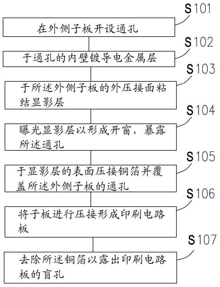
[0032] see Figure 1 to Figure 8 , a method for manufacturing a printed circuit board is provided for an embodiment of the present invention, specifically, the method includes the following steps:

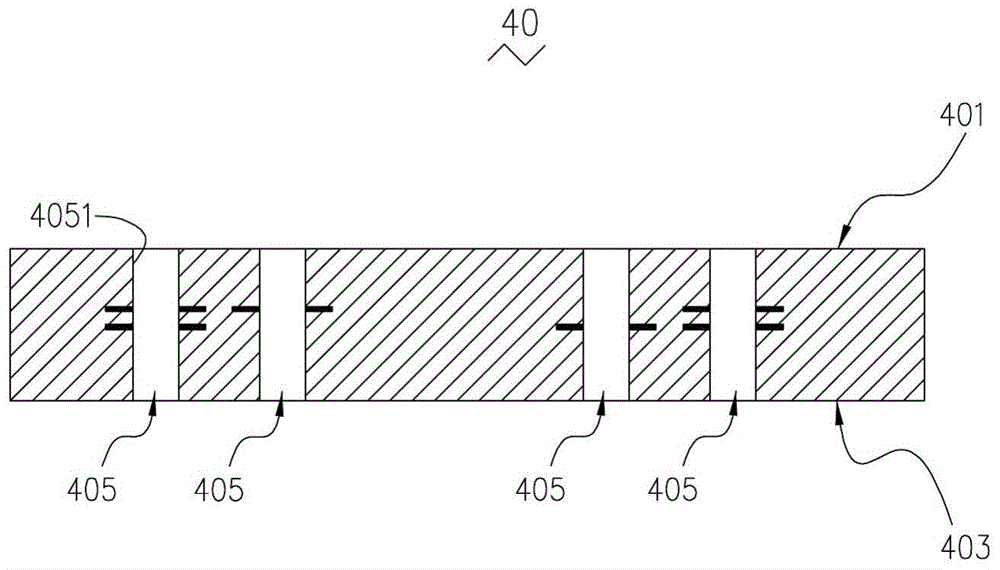
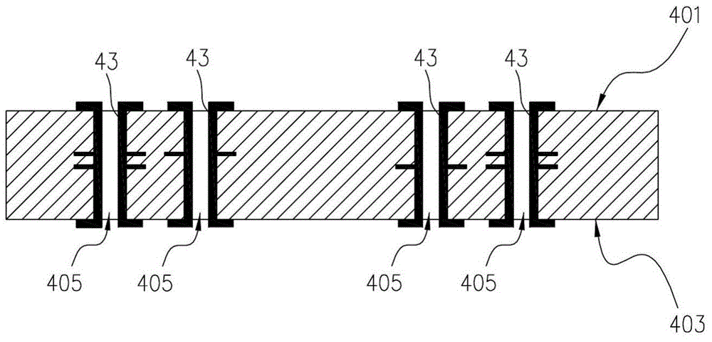
[0033] Step S101, such as figure 2 As shown, at least one through hole 405 is opened on one of the two outer sub-boards 40, and the through hole 405 passes through the outer crimping surface 401 and the inner crimping surface 403 of the outer sub-board 4...


PUM


Abstract

The invention provides a printed circuit board, which comprises a plurality of sub boards, wherein the plurality of sub boards comprise two outer side sub boards, the two outer side sub boards are respectively positioned at the two outer sides of the printed circuit board, at least one through hole is formed in at least one outer side sub board, a through hole penetrates through the outer pressing connection surface and the inner pressing connection surface of each outer side sub board, the outer pressing connection surface is bonded with a developing layer, the developing layer is provided with an open window, a hole opening and a hole disc of each through hole are exposed out of the corresponding open window, the developing layer is made of developing materials, and the developing materials are in a dry film form. The printed circuit board has the advantages that the developing layer is boned at each outer side sub board, so that a copper foil is bonded in the manufacture procedure of the printed circuit board, and the protection is formed on blind holes of the printed circuit board. Each developing layer has good stability, so the developing layer cannot easily flow into the blind holes of the printed circuit board, and the influence on the electric performance of the printed circuit board is avoided. The invention also provides a manufacturing method of the printed circuit board.

Description

technical field [0001] The invention relates to the field of electronic devices, in particular to a printed circuit board and a method for manufacturing the printed circuit board. Background technique [0002] With the development of science and technology, people have higher and higher requirements for the integration of printed circuit boards, so that the density of crimped blind holes on printed circuit boards is increasing. Correspondingly, the distance between crimped blind holes is getting more and more Small. [0003] Currently, pre-windowed prepreg combined with copper foil is usually used to protect the crimping blind holes of the sub-board against infiltration. The disadvantage of this technology is that the window opening area of ​​the prepreg is not easy to be accurately aligned with the blind hole, and the prepreg melts at a high temperature to form a flowing gel (referred to as "flowing glue"), which is easy to flow into the blind hole. Affects the electrical...

Claims


Application Information

Patent Timeline
Patent Type & Authority Applications(China)
IPC IPC(8): H05K1/02H05K1/11H05K3/42H05K3/46
Inventor 田清山高峰
Owner HUAWEI TECH CO LTD
Why Eureka
Try Eureka