Process method for improving two-dimensional graph resolution

A process method and two-dimensional graphics technology, applied in the field of semiconductor manufacturing, can solve problems such as shortening of wire ends and rounding of corners

Active Publication Date: 2015-06-10
SHANGHAI HUALI MICROELECTRONICS CORP
View PDF5 Cites 10 Cited by
  • Summary
  • Abstract
  • Description
  • Claims
  • Application Information

AI Technical Summary

Problems solved by technology

see figure 1 as well as figure 2 , figure 1 for pre-designed graphics, figure 2 For the actually formed graphics, compare figure 1 as well as figure 2 It c

Method used


Image

  • Process method for improving two-dimensional graph resolution
  • Process method for improving two-dimensional graph resolution
  • Process method for improving two-dimensional graph resolution

Examples


Embodiment Construction

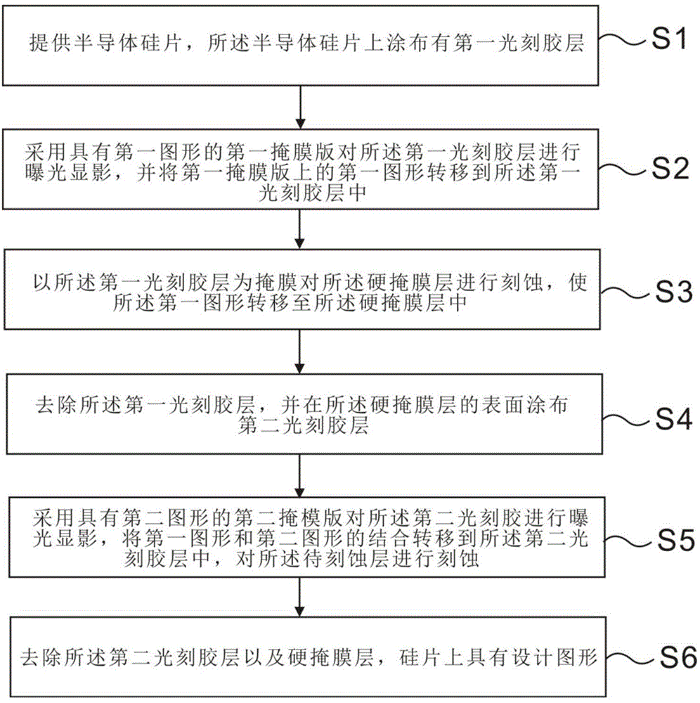
[0031] In order to make the content of the present invention clearer and easier to understand, the content of the present invention will be further described below in conjunction with the accompanying drawings. Of course, the present invention is not limited to this specific embodiment, and general replacements known to those skilled in the art are also covered within the protection scope of the present invention. Secondly, the present invention is described in detail by means of schematic diagrams. When describing the examples of the present invention in detail, for the convenience of explanation, the schematic diagrams are not partially enlarged according to the general scale, which should not be used as a limitation of the present invention.

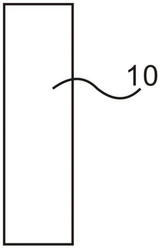
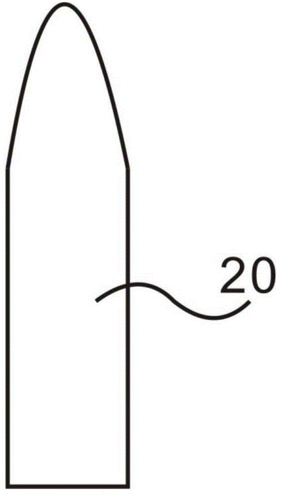
[0032] The above and other technical features and beneficial effects will be combined with the embodiments and the accompanying Figure 1 to Figure 10 The process method for improving the resolution of two-dimensional graphics of the ...


PUM


Abstract

The invention relates to the technical field of semiconductor technologies, and provides a process method for improving two-dimensional graph resolution. According to the method, a double-exposure mode is adopted, and for the region where circular beads are generated easily and shortened easily in a final design graph, in the first exposure process, a first graph of a first metal pattern plate is preprocessed to outwards extend by a certain distance; in the second exposure process, a second photoetching glue layer is coated, a second metal pattern plate is used for blocking a pre-extension region, the finally-formed graph is made to be consistent with the design graph through exposure etching, the phenomena that the graph generates corners and becomes round, and the line end is shortened are avoided, graph distortion is prevented, and the resolution of the two-dimension graph is improved.

Description

technical field [0001] The invention relates to the technical field of semiconductor manufacturing, in particular to a process method for improving the resolution of two-dimensional graphics. Background technique [0002] With the continuous improvement of semiconductor integrated circuit manufacturing technology and the continuous reduction of line width, the area of ​​semiconductor devices is becoming smaller and smaller. Semiconductor integrated circuits also have more comprehensive and powerful functions from the initial integrated circuits to large-scale integrated circuits, ultra-large-scale integrated circuits, and today's ultra-large-scale integrated circuits. Considering the constraints of unfavorable factors such as the complexity, long-term and high cost of process research and development, how to further increase the integration density of devices and reduce the chip area on the basis of existing technologies, so as to achieve as much as possible on the same sili...

Claims


Application Information

Patent Timeline
IPC IPC(8): G03F7/00H01L21/033
Inventor 顾婷婷季亮魏芳朱骏吕煜坤张旭昇
Owner SHANGHAI HUALI MICROELECTRONICS CORP
Why Eureka
Try Eureka