Touch liquid crystal display panel and touch liquid crystal display device

A technology for liquid crystal display panels and liquid crystal display devices, which is applied in optics, instruments, electrical and digital data processing, etc., can solve the problems of uneven deltaC at the edge and affect the touch accuracy at the edge, so as to improve the unevenness and enhance the touch. The effect of control precision

Inactive Publication Date: 2015-06-17
TCL CHINA STAR OPTOELECTRONICS TECH CO LTD +1
View PDF5 Cites 10 Cited by
  • Summary
  • Abstract
  • Description
  • Claims
  • Application Information

AI Technical Summary

Problems solved by technology

[0006] The object of the present invention is to provide a touch-control liquid crystal display panel and a touch-control liquid crystal display device, aiming to solve the problem that the delta C at the edge is not smooth because there is no corresponding sensor at the edge for comparison, which affects the precision of touch at the edge. degree of question

Method used


Image

  • Touch liquid crystal display panel and touch liquid crystal display device
  • Touch liquid crystal display panel and touch liquid crystal display device
  • Touch liquid crystal display panel and touch liquid crystal display device

Examples


Embodiment 1

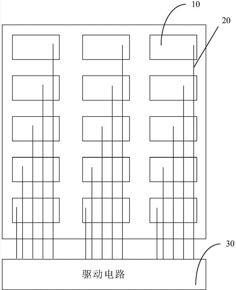
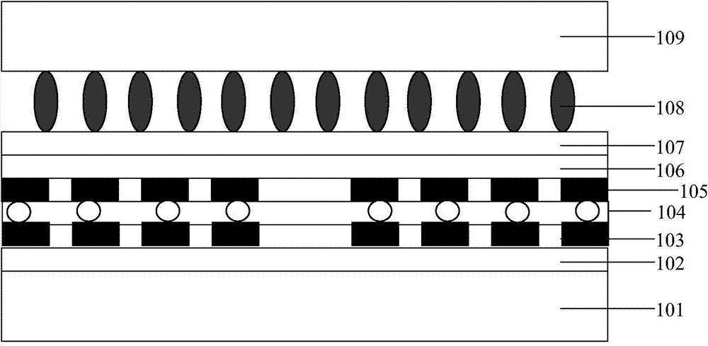
[0047] Please also refer to figure 2 and image 3 , is a schematic structural diagram of the touch liquid crystal display panel provided by the embodiment of the present invention; for the convenience of description, only the parts related to the embodiment of the present invention are shown.

[0048] The touch liquid crystal display panel includes: a first substrate 101, a TFT array layer 102, a common electrode layer 103, an insulating layer 104, a touch layer 105, a dielectric layer 106, and a pixel electrode layer 107 , a liquid crystal layer 108, and a second substrate 109; wherein, the TFT array layer 102 is disposed above the first substrate 101, the common electrode layer 103 is disposed above the TFT array layer 102, and the common The electrode layer 103 has a plurality of common electrodes; for example, the common electrode layer 103 has a plurality of common electrodes distributed in an array; the insulating layer 104 is arranged above the common electrode layer ...

Embodiment 2

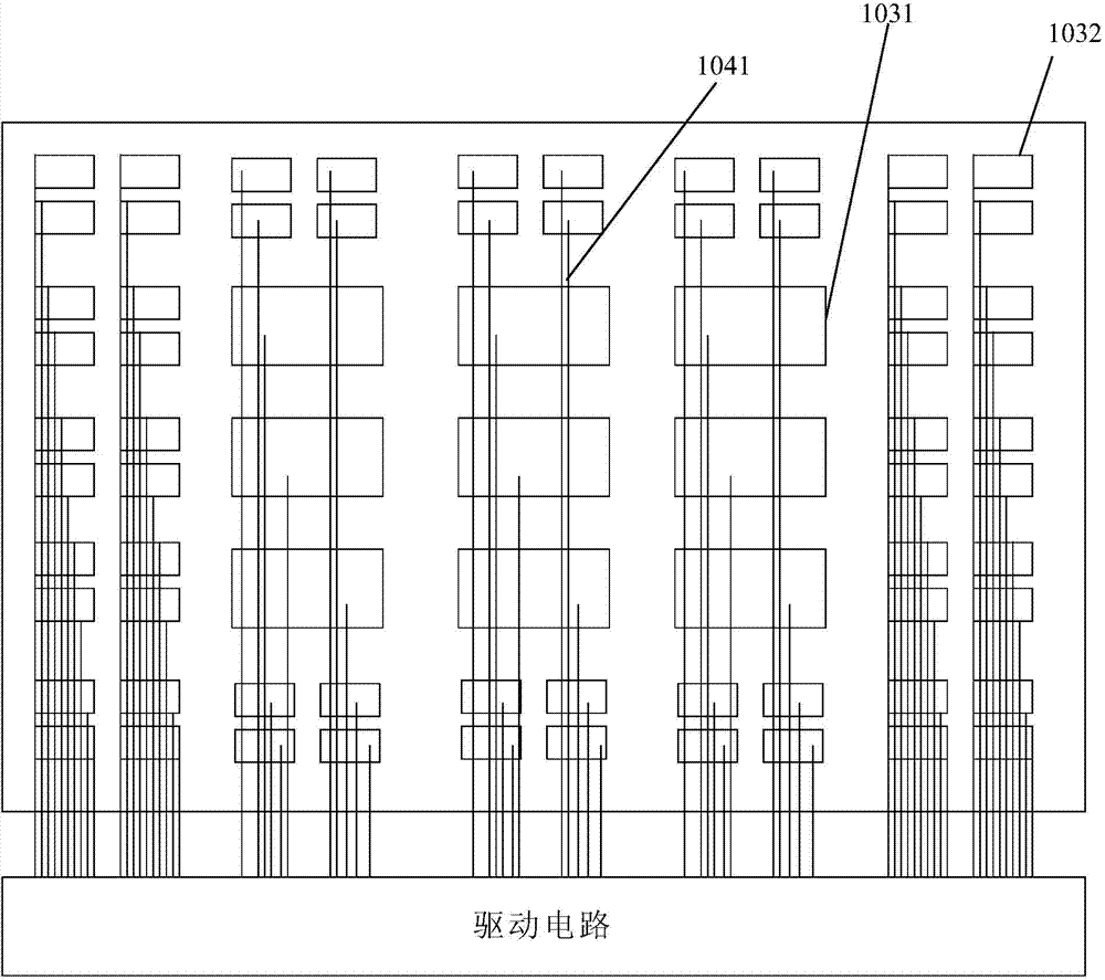
[0060] see Figure 4 , Figure 4 Another schematic diagram of the structure of the common electrode layer provided by the embodiment of the present invention; for the convenience of description, only the parts related to the embodiment of the present invention are shown. The second embodiment is similar to the first embodiment above, the difference is:

[0061] In the embodiment of the present invention, the shape of the peripheral common electrode 1032 is irregular. However, it can be understood that the peripheral common electrodes 1032 are randomly arranged in the edge region, as long as there is a small gap between the peripheral common electrodes 1032 and they are arranged closely together.

[0062] The embodiment of the present invention also provides a touch-control liquid crystal display device, the touch-control liquid crystal display device includes a touch-control liquid crystal display panel and a backlight module, and the touch-control liquid crystal display pan...


PUM


Abstract

The invention discloses a touch liquid crystal display panel comprising a first substrate, a TFT array layer, a common electrode layer, an insulating layer, a touch layer, a dielectric layer, a pixel electrode layer, a liquid crystal layer and a second substrate, wherein the common electrode layer comprises a plurality of common electrodes; the insulating layer is used for isolating the common electrode layer from the touch layer and is provided with a plurality of through holes; the touch layer is used for receiving touch signals; the touch layer comprises a plurality of touch lines, and the touch lines are connected with the corresponding common electrodes by virtue of corresponding through holes; the dielectric layer is used for isolating the touch layer and the pixel electrode layer; the second substrate is provided with a black matrix; the common electrodes comprise a plurality of central common electrodes positioned in a central area and a plurality of peripheral common electrodes positioned in an edge area; and under the same unit area, the number of the peripheral common electrodes in the edge area is more than the number of the central common electrodes in the central area. By adopting the touch liquid crystal display panel disclosed by the invention, the problem that delta C is unsmooth because the edges are lack of comparison capacitance can be solved, and the touch accuracy of the edges can be enhanced.

Description

【Technical field】 [0001] The present invention relates to the field of display technology, in particular to a touch liquid crystal display panel and a touch liquid crystal display device. 【Background technique】 [0002] With the increasingly fierce competition in the smart phone market, the structural design of thinner and lighter products has become one of the focuses of mobile phone manufacturers. , touch screen), panel manufacturers are committed to the research and development of product thinning solutions, and Full in-cell technology is considered to be the ultimate solution for touch technology thinning solutions. [0003] see figure 1 , which is a structural schematic diagram of a touch display panel provided in the prior art. The common electrodes 10 on the array substrate are patterned into a matrix checkerboard format, and the common electrodes 10 are connected to the drive circuit 30 through metal leads 20. Touch The driving circuit is designed in the way of tim...

Claims


Application Information

Patent Timeline
IPC IPC(8): G02F1/1333G02F1/1343G06F3/044
CPCG02F1/1333G02F1/13338G02F1/134309G06F3/0412G06F3/044
Inventor 谢剑星周诗博黄耀立
Owner TCL CHINA STAR OPTOELECTRONICS TECH CO LTD
Why Eureka
Try Eureka