Semiconductor film thickness measurement calibration standard sheet and manufacturing method thereof

A standard wafer, film thickness technology, applied in semiconductor devices, semiconductor/solid-state device testing/measurement, semiconductor/solid-state device components, etc., can solve the problem of high price, increase the risk of damage to standard wafers, and spend a lot of time and other problems to achieve the effect of improving work efficiency, reducing the probability of fragmentation and control efficiency, and saving expenses

Active Publication Date: 2015-06-17
SEMICON MFG INT (SHANGHAI) CORP
View PDF3 Cites 4 Cited by
  • Summary
  • Abstract
  • Description
  • Claims
  • Application Information

AI Technical Summary

Problems solved by technology

[0004] It can be seen from the above description; in the existing technology, multiple standard sheets are required to calibrate a measuring machine, and the current general standard sheets are relatively expensive, requiring a large amount of money to purchase and routinely test the standard sheets every year. In addition, during the calibration process, the measuring machin

Method used


Image

  • Semiconductor film thickness measurement calibration standard sheet and manufacturing method thereof
  • Semiconductor film thickness measurement calibration standard sheet and manufacturing method thereof
  • Semiconductor film thickness measurement calibration standard sheet and manufacturing method thereof

Examples


Embodiment Construction

[0059] In order to make the purpose, technical solution and advantages of the present invention more clear, the present invention will be further described in detail below with reference to the accompanying drawings and examples.

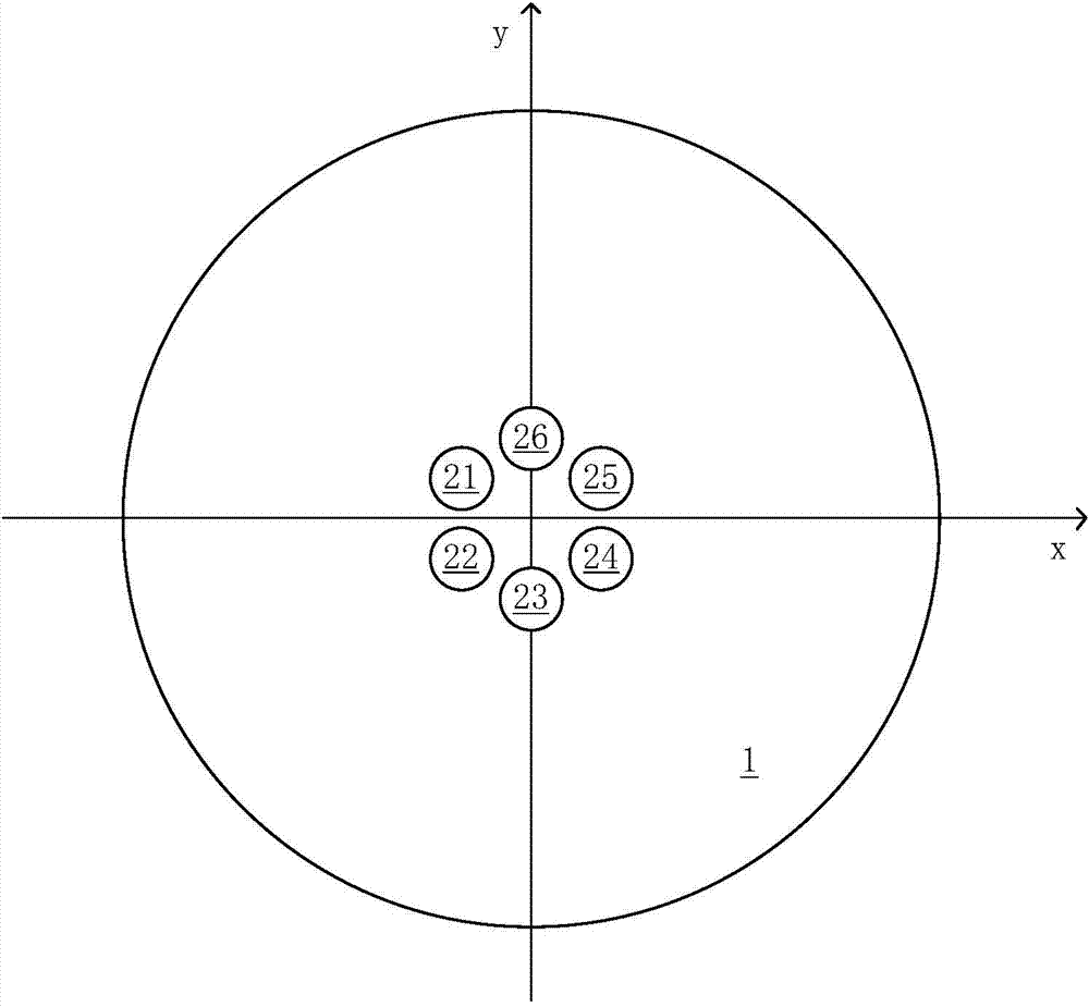
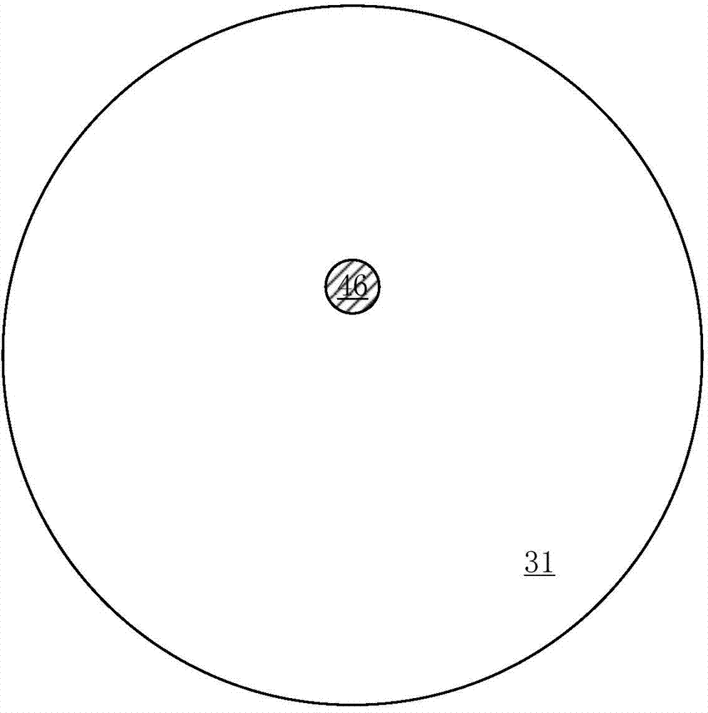
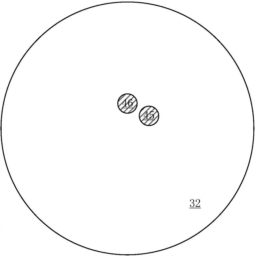
[0060] The semiconductor film thickness measurement calibration standard sheet provided by the present invention includes a wafer substrate and at least two pattern areas of different film thickness levels located on the surface of the wafer substrate. Wherein, the number of pattern areas can be adjusted according to the film thickness measuring machine and the need for film thickness measurement. Those skilled in the art can expand the pattern area of ​​the embodiment according to the introduction of the following embodiments combined with the existing technology in the field Or to reduce the number to the required number, the position of each pattern area on the wafer substrate can also be adjusted arbitrarily in combination with the introduction o...


PUM

PropertyMeasurementUnit
Diameteraaaaaaaaaa
Thicknessaaaaaaaaaa
Thicknessaaaaaaaaaa

Abstract

The invention discloses a semiconductor film thickness measurement calibration standard sheet and a manufacturing method thereof. The calibration standard sheet comprises a wafer substrate and at least two pattern regions which are located on the surface of the wafer substrate and are of different film thickness levels. Due to the fact that the pattern regions of the different thickness levels are formed on the same standard sheet, the same standard sheet can be adopted for calibrating multiple thickness levels. Compared with the prior art, the expense for purchasing the standard sheet can be saved, the measurement use rate of a film thickness measurement table used for a product is increased, the work efficiency of operators is improved, and meanwhile the wafer breakage probability and the management and control efficiency of a wafer of the standard sheet are reduced.

Description

technical field [0001] The invention relates to semiconductor testing technology, in particular to a calibration standard sheet used in semiconductor film thickness measuring equipment and a manufacturing method thereof. Background technique [0002] With the continuous development of semiconductor manufacturing technology, the role of measurement equipment is becoming more and more important. It is also extremely important to ensure the accuracy of semiconductor measurement. To ensure the accuracy of measurement, it is necessary to rely on standard plates to regularly calibrate the equipment. . [0003] Semiconductor production plants have various types of measurement machines (equipment), and the equipment for film thickness measurement requires thickness measurement calibration standard sheets. At present, a set of thickness measurement calibration standard sheets is composed of several wafers, each wafer is used to calibrate a thickness value, and a layer of carbon diox...

Claims


Application Information

Patent Timeline
IPC IPC(8): H01L23/544H01L21/66
Inventor 刘媛娜尹正朝周欣洁
Owner SEMICON MFG INT (SHANGHAI) CORP
Why Eureka
Try Eureka