Array substrate, display panel and display device

An array substrate and substrate technology, applied in the field of touch display, can solve the problem of low touch precision, achieve high touch precision and reduce coupling capacitance

Active Publication Date: 2015-06-24
SHANGHAI TIANMA MICRO ELECTRONICS CO LTD +1
View PDF3 Cites 22 Cited by
  • Summary
  • Abstract
  • Description
  • Claims
  • Application Information

AI Technical Summary

Problems solved by technology

However, the existing self-capacitive touch display devices have low touch accuracy

Method used


Image

  • Array substrate, display panel and display device
  • Array substrate, display panel and display device
  • Array substrate, display panel and display device

Examples


Embodiment Construction

[0021] The following will clearly and completely describe the technical solutions in the embodiments of the present invention with reference to the accompanying drawings in the embodiments of the present invention. Obviously, the described embodiments are only some, not all, embodiments of the present invention. Based on the embodiments of the present invention, all other embodiments obtained by persons of ordinary skill in the art without making creative efforts belong to the protection scope of the present invention.

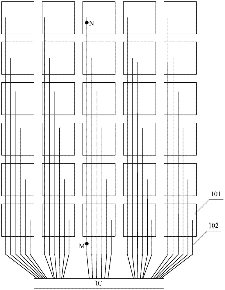
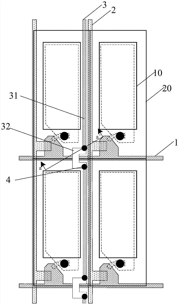
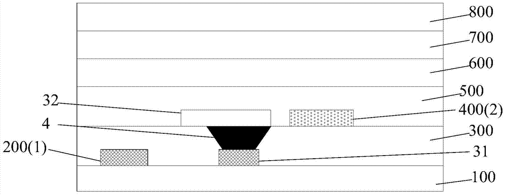
[0022] As mentioned in the background, the existing self-capacitive touch display devices have low touch accuracy. The inventors found that the main reason for this problem is that the distance between the conductive layer where the touch lead wire is located and the conductive layer where the touch electrode is located is small, and there is a large coupling capacitance between the touch lead wire and the touch electrode that it passes through. As a result, t...


PUM


Abstract

The invention discloses an array substrate, a display panel and a display device. The array substrate comprises multiple gate lines, multiple data lines and multiple touch leads; the extension directions of the touch leads are parallel to the extension directions of the data lines, each touch lead comprises multiple lead portions and multiple connecting portions, the lead portions and the gate lines are arranged on the same layer, and each lead portion is arranged between two adjacent gate lines; the connecting portions and the lead portions are located at different conducting layers, and each connecting portion connects two lead portions through a via hole. Each touch lead is arranged to be a line provided with the multiple lead portions and the multiple connecting portions, the lead portions and the gate lines are arranged at the same layer, the two lead portions are in electric connection with each other through a via hole connection mode, the distance between the conducting layer of the lead portions and the conducting layer of touch electrodes are enlarged, and coupling capacitance between the lead portions and touch electrodes corresponding to positions of the lead portions is reduced, and it is guaranteed that the touch accuracy of the display device is high.

Description

technical field [0001] The present invention relates to the field of touch display technology, and more specifically, relates to an array substrate, a display panel and a display device. Background technique [0002] In the initial stage of the development of the touch display, the touch display panel is formed by laminating the touch panel and the display panel to realize the touch display. The touch panel and the display panel need to be prepared separately, the cost is high, the thickness is relatively large, and the production efficiency is low. [0003] With the development of self-capacitive touch display integration technology, the common electrode of the array substrate in the display panel can also be used as the touch sensing electrode for self-capacitive touch detection, and the touch can be performed in time-sequence through time-sharing driving Control and display control can realize touch and display functions at the same time. In this way, the touch sensing ...

Claims


Application Information

Patent Timeline
Patent Type & Authority Applications(China)
IPC IPC(8): G06F3/041
CPCG02F1/13338G02F1/136286G06F3/0412G06F3/04164G06F3/0443
Inventor 杜凌霄姚绮君
Owner SHANGHAI TIANMA MICRO ELECTRONICS CO LTD
Why Eureka
Try Eureka