IC card packaging device and method
A packaging device and packaging method technology, applied in electrical components, semiconductor/solid-state device manufacturing, circuits, etc., can solve problems such as shrinkage deformation, poor user sensory experience, and affecting the aesthetics of the card surface.
- Summary
- Abstract
- Description
- Claims
- Application Information
AI Technical Summary
Problems solved by technology
Method used
Image
Examples
Embodiment Construction
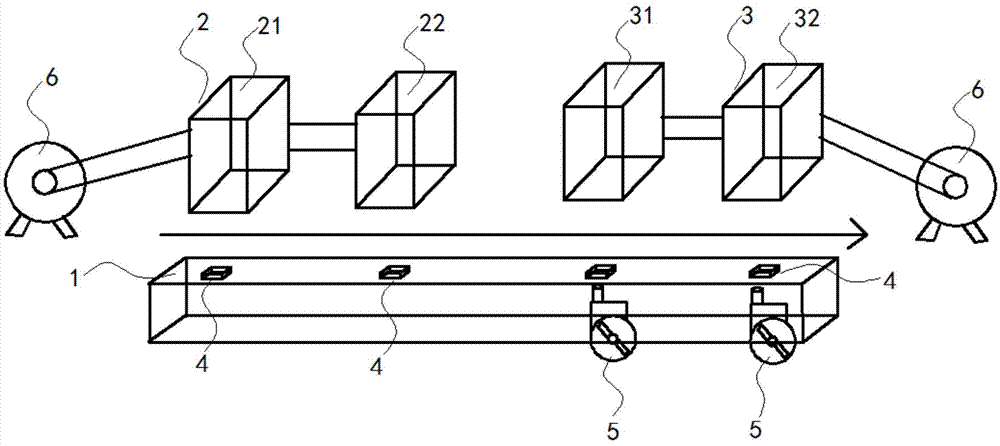
[0038] In order to describe the technical content, structural features, achieved goals and effects of the present invention in detail, the following will be described in detail in conjunction with the embodiments and accompanying drawings.
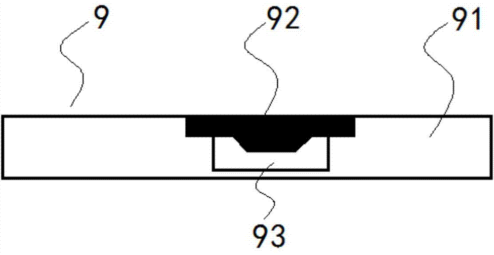
[0039] see figure 2 , is the IC card schematic diagram after encapsulation; Described IC card 9 comprises plastic card base 91 and IC card chip 92, from figure 2 It can be seen from the figure that when the chip is embedded in the card body of the plastic card base, it cannot completely fill the chip slot on the plastic card base, so there is still a certain space in the chip slot on the plastic card base below the IC card chip 92. Empty area 93. In this way, during the packaging process of the IC card, due to the existence of the avoidance area, the plastic card base is prone to shrinkage and deformation when it is cooled, which leads to the back of the packaged plastic card base (that is, the other side opposite to the chip side) on t...
PUM
| Property | Measurement | Unit |
|---|---|---|
| Diameter | aaaaa | aaaaa |
Abstract
Description
Claims
Application Information


