
Optical laminate for front surface of in-cell touch panel liquid crystal element and in-cell touch panel liquid crystal display device using same

一种液晶显示装置、光学叠层体的技术,应用在光学、光学元件、偏振元件等方向,能够解决厚度或重量增加等问题,达到防止白浊的效果

Active Publication Date: 2018-05-29
DAI NIPPON PRINTING CO LTD
View PDF15 Cites 0 Cited by
  • Summary
  • Abstract
  • Description
  • Claims
  • Application Information

AI Technical Summary

Problems solved by technology

[0003] In the external type, the liquid crystal display device and the touch panel are manufactured separately and then integrated, so even if one of them is defective, the other can be used, and the yield is excellent, but there are problems of increased thickness and weight

Method used


Image

  • Optical laminate for front surface of in-cell touch panel liquid crystal element and in-cell touch panel liquid crystal display device using same
  • Optical laminate for front surface of in-cell touch panel liquid crystal element and in-cell touch panel liquid crystal display device using same
  • Optical laminate for front surface of in-cell touch panel liquid crystal element and in-cell touch panel liquid crystal display device using same

Examples


Embodiment 1

[0239] (1) Production of surface protective film

[0240] [Adjustment of the coating solution for the cured layer for the outermost surface]

[0241] The pentaerythritol triacrylate (Nippon Kayaku Co., PET-30), polymer-containing acrylate resin (Arakawa Chemical Co., Beamset DK-1) and silica particle dispersion (JSR Co., KZ6406) The solid content of 3 components was added to methyl isobutyl ketone so that it might become 50 parts, 25 parts, and 25 parts in order, and it stirred, and obtained the solution a.

[0242] Next, with respect to 100 parts of the solid content of the solution a, 7 parts by mass of a photopolymerization initiator (manufactured by BASF Japan, Irgacure 184) and 1.5 parts by mass of a photopolymerization initiator (manufactured by BASF Japan, Lucirin TPO) were added and stirred and This was dissolved to prepare a solution b having a final solid content of 40% by mass.

[0243] Next, 0.4 parts of a leveling agent (product name MegaFuck RS71, manufactured by DIC Co...

Embodiment 2

[0257] On the conductive layer (first conductive layer) of Example 1, except that the second conductive layer was formed by the following method, the same procedure as in Example 1 was carried out to produce an optical laminate.

[0258] (Formation of the second conductive layer)

[0259] Pentaerythritol triacrylate (PETA) and HRAG acrylic (25) MIBK (thermoplastic resin) manufactured by DNP Fine Chemicals Co., Ltd. were added to methyl ethyl ketone (MEK) so that the solid content of the above 2 components became 70 parts and 30 parts. ) / Isopropanol (IPA) mixed solvent and stirred and dissolved to obtain solution e.

[0260] Next, to 100 parts of the solid content of the solution e, 4 parts by mass of a photopolymerization initiator (manufactured by BASF Japan, Irgacure 184) and 0.2 part of a leveling agent (manufactured by Dainichi Seiki Kogyo Co., Ltd., 10-301 (TL)) were added And stirring to prepare solution f.

[0261] Next, to 100 parts by mass of the resin component of the solut...

Embodiment 3

[0264] In Example 1, the conductive layer (first conductive layer) was formed on the surface protective film instead of the retardation film, and the conductive layer side of the surface protective film and the polarizing film were bonded together, except that it was the same as in Example 1. Operation to produce an optical laminate. In addition, regarding Example 3, before bonding a surface protection film and a retardation film, the same grounding process as Example 1 was performed.


PUM

PropertyMeasurementUnit
particle diameteraaaaaaaaaa
glass transition temperatureaaaaaaaaaa

Abstract

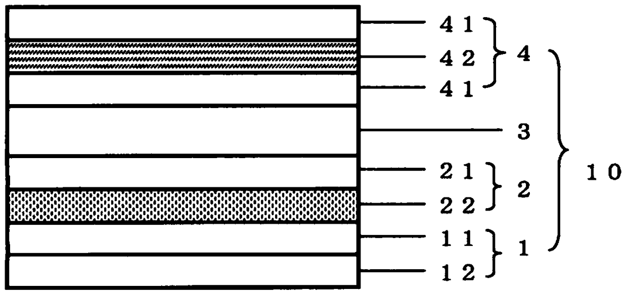
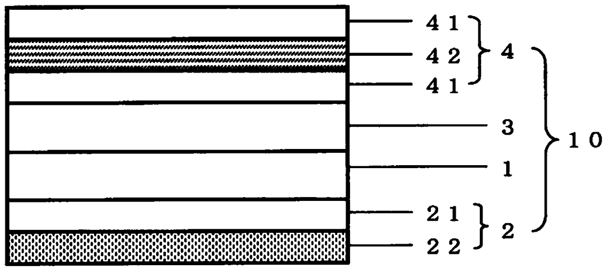
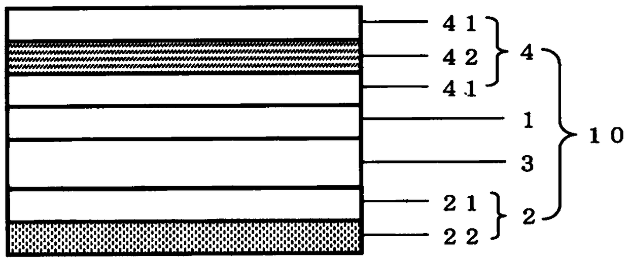
The optical laminate for a front surface of an in-cell touch panel liquid crystal element comprises a phase difference plate, a polarizing film, and a surface protective film in this order, and further comprises a conductive layer. The surface protective film has optical anisotropy that scatters linear polarized light emitted from the polarizing film, and a thickness of the optical laminate is in a range of 90 μm to 450 μm.

Description

Technical field [0001] The present invention relates to an optical laminate for the front surface of an in-cell touch panel liquid crystal element and an in-cell touch panel type liquid crystal display device using the same. Background technique [0002] In recent years, portable liquid crystal terminals represented by smartphones and other liquid crystal display devices have been equipped with touch panel functions. For liquid crystal display devices equipped with such a touch panel function, currently the mainstream is an external type in which a touch panel is mounted on the liquid crystal display device. [0003] The external type is integrated after manufacturing the liquid crystal display device and the touch panel separately. Therefore, even if one of them is defective, the other can be used. The yield is excellent, but there is a problem of increased thickness or weight. [0004] As a device that solves the problem (thickness or weight) of such an external type, a so-called ...

Claims


Application Information

Patent Timeline
Patent Type & Authority Patents(China)
IPC IPC(8): G02B5/30B32B7/02G02F1/1333G02F1/1335G02F1/13363G02F1/1343G06F3/041
CPCB32B2551/00G02B5/3033G02F1/13338G02F1/133528G02F1/13363G02F2201/50G02B1/14G02B5/3083B32B2457/202G02B5/3041
Inventor 恒川雅行
Owner DAI NIPPON PRINTING CO LTD
Learn More