Touch screen and manufacture method thereof

A manufacturing method and touch screen technology, applied in the field of touch screens, can solve the problems of low processing efficiency, slow aerosol printing speed, cumbersome yellow light lithography process, etc., and achieve the effect of improving processing efficiency and simplifying the processing process

Inactive Publication Date: 2015-07-01
HONG FU JIN PRECISION IND (SHENZHEN) CO LTD +1
View PDF0 Cites 4 Cited by
  • Summary
  • Abstract
  • Description
  • Claims
  • Application Information

AI Technical Summary

Problems solved by technology

Bridge metal wires are generally formed by etching through the lithography process, but the lithography process is relatively cumbersome; or

Method used


Image

  • Touch screen and manufacture method thereof
  • Touch screen and manufacture method thereof
  • Touch screen and manufacture method thereof

Examples


Example Embodiment

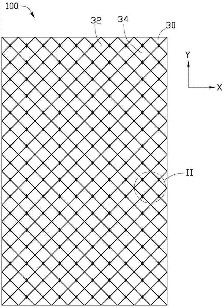
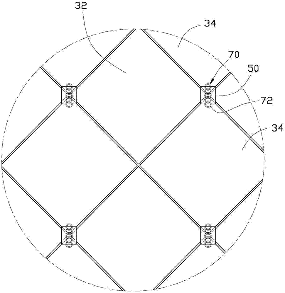
[0014] Please also refer to figure 1 and figure 2 The touch screen 100 according to the embodiment of the present invention includes a substrate 10 , a conductive layer 30 formed on the surface of the substrate 10 , a plurality of insulating layers 50 and a plurality of bridging lines 70 . In the embodiment of the present invention, the substrate 10 is made of a transparent insulating material, which may be made of transparent glass, polyethylene terephthalate (PET) and other materials.

[0015] The conductive layer 30 is formed with a plurality of first electrodes 32 and a plurality of second electrodes 34 arranged roughly in a matrix, the plurality of first electrodes 32 and the plurality of second electrodes 34 are insulated from each other, and the first electrodes 32 and the second electrodes 34 are arranged alternately with each other in columns. In the embodiment of the present invention, both the first electrode 32 and the second electrode 34 are approximately diamo...


PUM

PropertyMeasurementUnit
Widthaaaaaaaaaa
Diameteraaaaaaaaaa
Line widthaaaaaaaaaa

Abstract

The invention discloses a manufacture method of a touch screen. The manufacture method comprises the following steps: forming a conducting layer on a substrate; etching the conducting layer to form a plurality of first electrodes and a plurality of second electrodes, wherein the first electrodes and the second electrodes are roughly arranged in a matrix way, are mutually insulated and are arranged at intervals; forming a plurality of insulating layers on the conducting layer, wherein each insulating layer covers the corners of two adjacent first electrodes arranged in the same row arranged along a first direction and the corners of two adjacent second electrodes arranged in the same line arranged in a second direction; and adopting an ink jet printing method to form a plurality of conducting rings which are mutually connected in series on the corresponding insulating layer. The invention also provides the touch screen which adopts the manufacture method. The manufacture method has the advantages of being simple in manufacture procedures and high in processing efficiency.

Description

technical field [0001] The invention relates to a touch screen, in particular to a touch screen with a single conductive layer and a manufacturing method thereof. Background technique [0002] Touch screens are widely used, and touch screens with a single-layer indium tin oxide (Single Indium Tin Oxide, SITO) structure have broader application prospects due to their thin thickness and low manufacturing cost. A SITO touch screen generally includes a substrate, and an indium tin oxide film formed on the substrate. The indium tin oxide film forms a plurality of first electrodes and a plurality of second electrodes roughly arranged in a matrix through etching and other methods. A plurality of second electrodes and a plurality of first electrodes are arranged at intervals. The plurality of first electrodes in the same row in the first direction are electrically connected. The plurality of second electrodes are insulated. In order to electrically connect the plurality of second ...

Claims


Application Information

Patent Timeline
IPC IPC(8): G06F3/041
Inventor 吴景扬赵天行
Owner HONG FU JIN PRECISION IND (SHENZHEN) CO LTD
Why Eureka
Try Eureka